AR-P 3200 series thick positive photoresist
High film thickness for electroplating and microsystem
…
AR-P 3200 series product brief 產品說明
AR-P 3200 系列,產品為正型厚膜光阻,黃光圖案尺寸精確,邊緣垂直度高,適合電鍍與微機電系統製程。
目前產品依配方與厚度範圍有如下序號:
…
Packing & shipping 產品包裝與出貨
packing 產品包裝
✅ 250 ml/瓶
✅ 1 L/瓶
其它包裝可依需求研擬增加
shipping 產品出貨
✅ 2 – 4 週。德國運出。(AR-P 3250)
其它序號目前無固定生產排程,需先詢問。
GHS 標識
…
Product features 產品特性
- broadband UV, i-line, g-line
曝光波長: 寬頻紫外線, i-line (365nm) , g-line (436nm) - high photosensitivity, high resolution
高敏感度,高解析度 - profiles with high edge steepness dimension accuracy
黃光圖案尺寸精確,邊緣垂直度高 - plasma etch resistant, electroplating-stable
耐電漿蝕刻. 電鍍製程穩定 - AR-P 3210 film thickness up to 40um/AR-P 3250 film thicknesses up to 20 μm
AR-P 3210 膜厚最高可達 40um/AR-P 3250膜厚最高可達20um - AR-P 3220 transparent for thick films up to 100 μm in multiple coating steps, 100μm development in one step
AR-P 3220 透明膜厚經多次疊加塗佈可達100um,僅需單次顯影 - combination of novolac and naphthoquinone diazide
主要成份為酚醛樹酯及叠氮基萘醌 - safer solvent PGMEA
使用較安全溶劑丙二醇甲醚醋酸酯
…
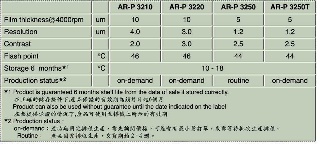
Product properties 產品物性
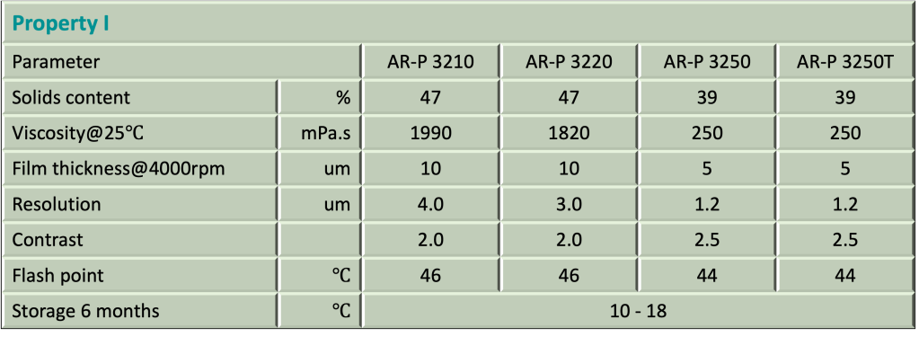
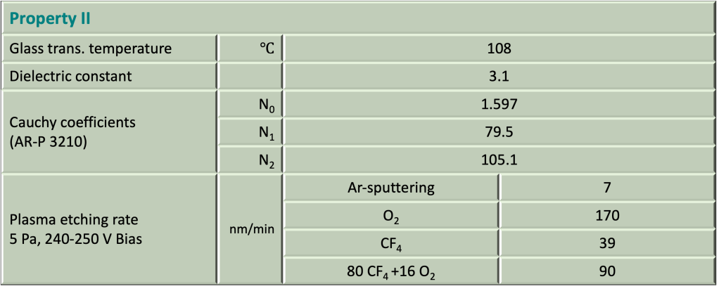
…
AR-P 3200 series Spin curve 塗佈曲線
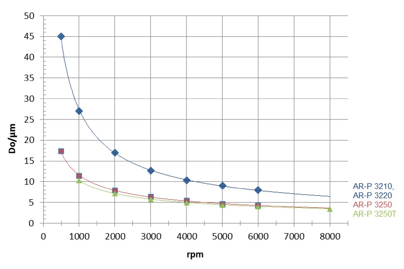
…
Structure and resolution 結構與解析度
Structure resolution
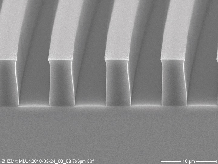
AR-P 3210 Film thickness 12 μm Resist structures 4 μm
Resist structure
AR-P 3220 Film thickness 25 μm
…
Process baseline 製程參數
This diagram shows exemplary process steps for AR-P 3200 series resists. All specifications are guideline values which must be adapted to own specific conditions. For further information on processing, 👉“ Detailed instructions for optimum processing of photoresists”. For recommendations on wastewater treatment and general safety instructions, 👉”General product information on Allresist photoresists”.
表列為AR-P 3200系列產品製程參數的範例。所有參數為參考值,使用者應依設備環境實際狀況加以調整。
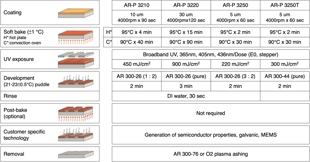
Process for the film thickness > 40um
Coating
Coating should be performed in two or several steps using the same procedure. After a low initial spin speed (30 s), a main spin speed of 250 – 500 rpm for at least 2-5 min should be chosen. A brief subsequent spinning off at 600 – 800 rpm for 5 s reduces edge bead formation.
塗佈
建議採用兩次或多次同參數的累加塗佈。 先以30秒低轉速讓光阻分佈於基板,隨後主轉速250 – 500轉約2 – 5分鐘。 最後提高轉速至600-800轉約5秒以減少邊緣隆起形成。
Tempering
Tempering should be performed in 2 steps:
1. 75 °C, 5 min hot plate or 70 °C, 30 min convection oven;
2. 90 °C, 20 min hot plate or 90 °C, 80 min convection oven. After tempering, a slow cooling is recommended to avoid stress cracks.
軟烤
建議兩階段軟烤以乾燥厚膜光阻:
1. 75℃ x 5min 熱板,或 70℃ x 30 min對流烤箱.
2. 90℃ x 20 min 熱板或90℃ x 80 min對流烤箱. 冷卻應緩慢降溫以避免應力造成裂痕.
Development recipe
…
Reference data 參考資料
Sensitivity vs. duration of the soft bake
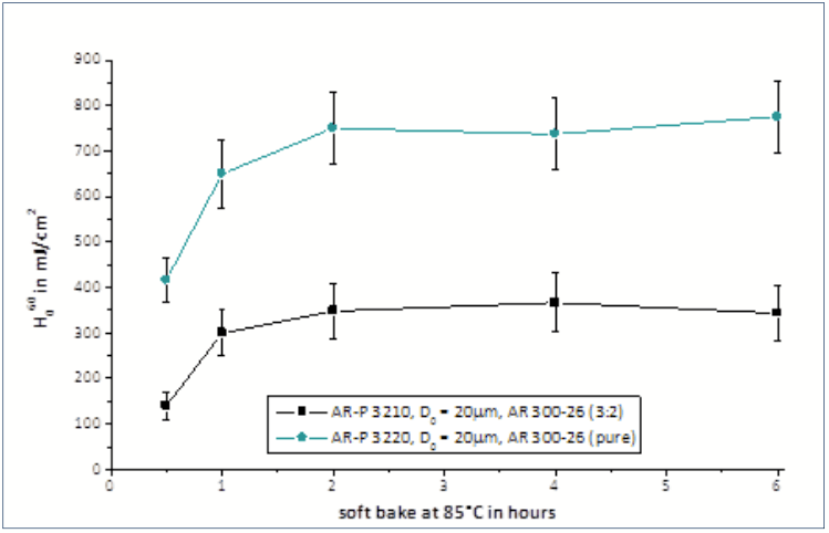
After 2 hours, the sensitivity remains more or less constant (broadband UV, resist thickness 20 μm).
Residual solvent after tempering
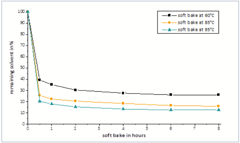
After a bake at 95 °C, approx. 7 % of the solvent remain in the layer (initial solids content: 47 %)
Sensitivity in different developers
Film thickness 20 µm, soft bake 85 °C, 1 h convection oven, bb UV
Dark erosion in different developers
Erosion corresponding to determined sensitivities
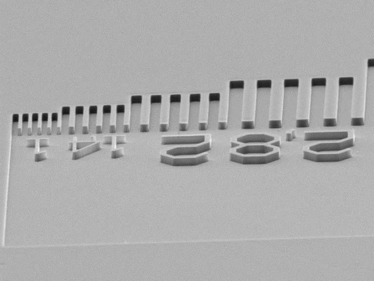
Grey tone mask lithography
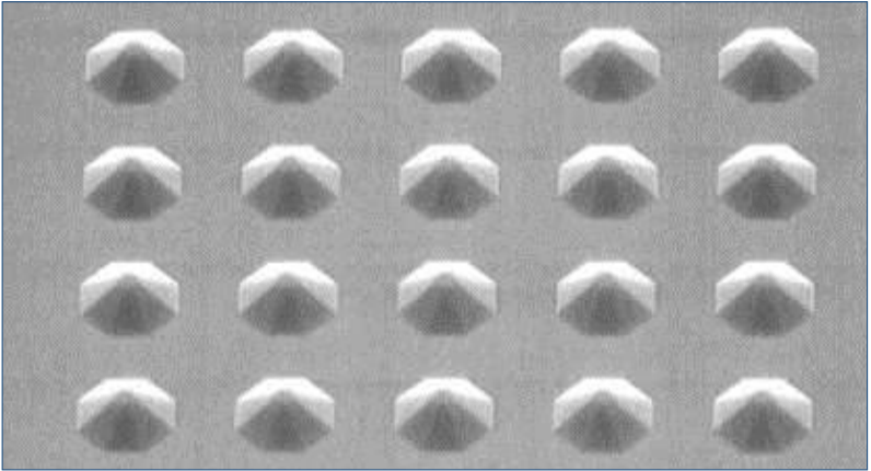
28 µm-high 3D pyramids with AR-P 3220
Photolysis of photo-active compound (PAC)
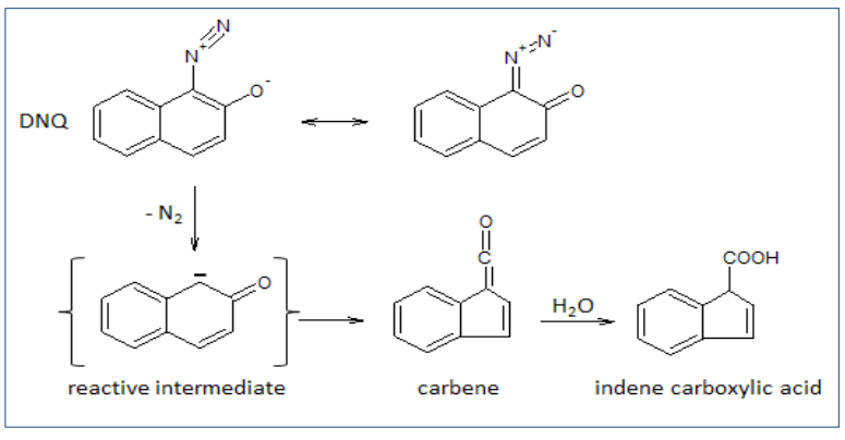
Chemical reaction for bleaching and full exposure of the layer (Süss reaction)
The transparency of AR-P 3220 is higher as compared to AR-P 3210, due to the lower concentration of the PAC. The gradation is accordingly relatively low. This fact can be used for the fabrication of three-dimensional structures using grey tone masks with AR-3220. Different exposure doses will result in different resist film thicknesses.
AR-P 3220由於感光劑(PAC)含量比AR-P 3210低,因此比較透明。階度(gradation)也比較低. 此特性可應用於具立體結構的灰階光罩。
不同曝光劑量會形成厚度的光阻結構。
…
