AR-P 3100 series positive photoresist
Adhesion enhanced positive photoresist

AR-P 3100 series positive photoresist
Adhesion enhanced positive photoresist
…
AR-P 3100 series product brief 產品說明
AR-P 3100 系列,產品配方強化與基板介面的接著度,適合各類精密微影製程的正型阻劑。
目前產品依配方與厚度範圍有如下序號:
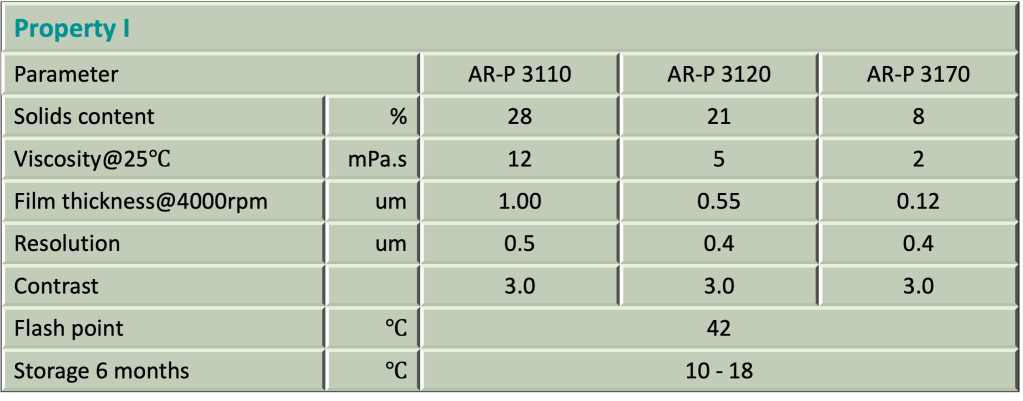
| Property |
| AR-P 3110 | AR-P 3120 | AR-P 3170 |
| Film thickness@4000rpm |
| 1 um | 0.55 um | 0.12 um |
| Resolution |
| 0.5 um | 0.4 um | 0.4 um |
| Contrast |
| 3.0 |
| Flash point |
| 46 ℃ |
| Storage 6 months*1 |
| 10 – 18 ℃1 |
| Production status*2 |
| routine1 |
- Product is guaranteed 6 months shelf life from the date of sale if stored correctly.
在正確儲存條件下,產品保證的有效期限為銷售日起6個月。
Product can also be used without guaranteed until the date indicated on the label.
在無提供保證的情況下,產品可使用至標籤上所示的有效期。 ↩︎ - Product status:
routine:產品固定排程生產,交貨期約2-4週。
on-demand:產品無固定排程生產,需先詢價。可能有最小訂購量(MOQ)或需待批次生產排程。 ↩︎
…
Packing & shipping 產品包裝與出貨
packing 產品包裝
✅ 250 ml/瓶
✅ 1 L/瓶
其它包裝可依需求研擬增加
shipping 產品出貨
✅ 2 – 4 週。德國運出。
本產品原廠為德國ALLRESIST GmbH. 瀏覽原廠網頁請按原廠標識。
This product is developed and produced by ALLRESIST GmbH.
Click logo to visit pricipal’s website.
…
Product features 產品特性
- broadband UV, i-line, g-line
曝光波長: 寬頻紫外線, i-line (365nm) , g-line (436nm) - high photosensitivity, high resolution
高敏感度,高解析度 - strong adhesion to critical glass/chromium surfaces for extreme stresses during wet-chemical etching processes
對玻璃,鉻等介面接著度良好,適合濕蝕刻製程 - for the production of CD masters and lattice structures
適合CD母片及各式點陣結構 - AR-P 3170 also suitable for laser interference lithography
AR-P 3170可用於雷射干涉微影 - plasma etching resistant
耐電漿蝕刻 - combination of novolac and naphthoquinone diazide
主要成份為酚醛樹酯及叠氮基萘醌 - safer solvent PGMEA
使用較安全溶劑丙二醇甲醚醋酸酯
…
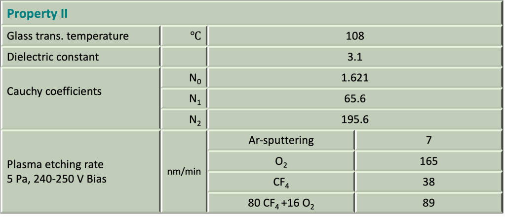
Product properties 產品物性
…
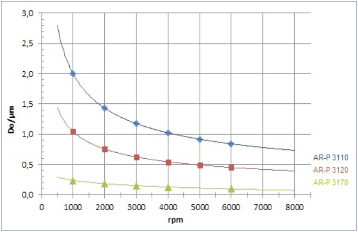
AR-P 3100 series Spin curve 塗佈曲線
…
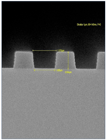
Structure and resolution 結構與解析度
Structure resolution
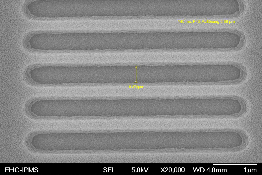
AR-P 3120:
Film thickness 0.6 μm Resist structures 0.38 μm L/S
Resist structure
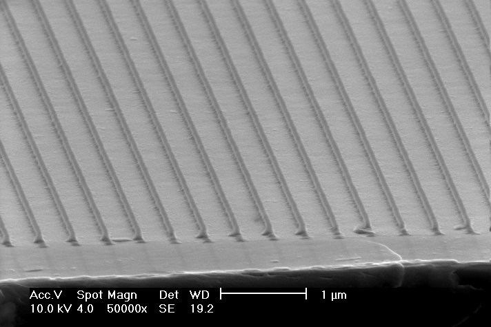
AR-P 3170:
70-nm-lines generated by laser interference lithography
…
Process baseline 製程參數
This diagram shows exemplary process steps for AR-P 3100 resists. All specifications are guideline values which must be adapted to own specific conditions. For further information on processing, 👉“ Detailed instructions for optimum processing of photoresists”. For recommendations on wastewater treatment and general safety instructions, 👉”General product information on Allresist photoresists”.
表列為AR-P 3100系列產品製程參數的範例。所有參數為參考值,使用者應依設備環境實際狀況加以調整。
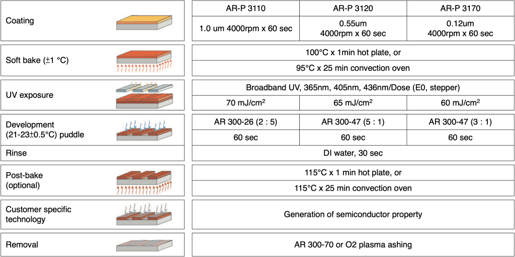
Development recipe
…
Reference data 參考資料
Linearity
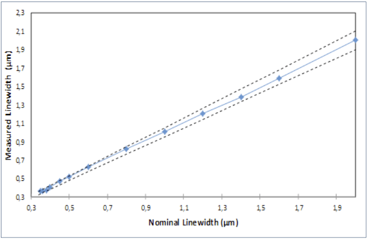
Up to a structure width of 0.38, a very good agreement is obtained. REM measurement: Thickness 560 nm, i-line stepper (NA: 0.65 NA), Developer AR 300-47 1 : 1.
Optimum exposure dose
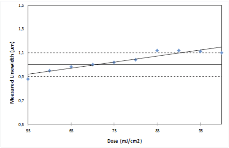
Underexposure leads in the case of complete development (more than 55 ml/cm2) to narrower trenches, while overexposure results in a widening of trenches.
Focus variation
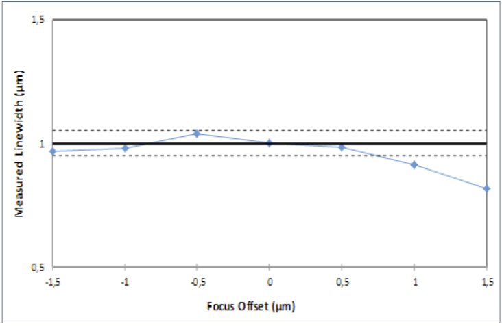
The intended structure sizes can here be realized by varying the focus between -1.5 to 0.8 (parameter see graphic linearity).
Focus variation (with and without PEB)
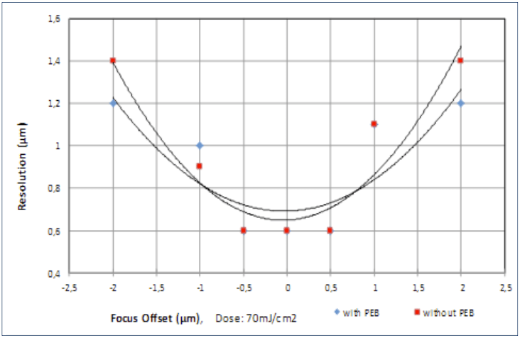
Without PEB, a higher resolution is obtained since the focus curve is steeper (PEB, 90 °C, 60 s).
Optimum exposure dose
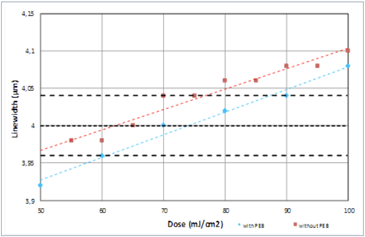
Optimum dose, with hard bake (110 °C) and without hard bake. The additional hard bake requires 15 % more light (PEB, 90 °C, 60 s).
Thermal properties of resist structures
Untempered

Hard bake 115℃
Contents are base on ALLRESIST product TDS.
Click logo below to link to ALLRESIST AR-P 3100 series product page .
內容取材自原廠產品技術資料,連結原廠請按下方標識。
