AR-N 4340 Negative Tone Chemically Amplified photoresist
high sensitive negative resist for the production of integrated circuits
…
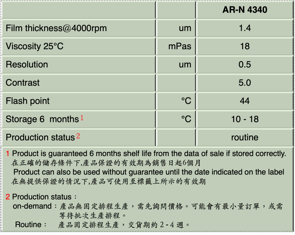
AR-N 4340 product brief 產品說明
AR-N 4340 為化學增幅型,高敏感度負型光阻,適合各類次微米(sub-um)電路運用。
產品基本資料如下:
…
Packing & shipping 產品包裝與出貨
packing 產品包裝
✅ 250 ml/瓶
✅ 1 L/瓶
其它包裝可依需求研擬增加
shipping 產品出貨
✅ 2 – 4 週。德國運出。
❎ 1 週。 國內庫存。
(本產品暫無國內庫存)
…
Product features 產品特性
- i-line, g-line
曝光波長: i-line (365nm) , g-line (436nm) - highest sensitivity, excellent resolution
高敏感度,高解析度 - good adhesion, high contrast, chemically enhanced
化學增幅型,具高對比,與基板黏著度良好 - undercut profiles (lift-off) are possible
可調整成下切型圖案, 用於懸浮剝離製程 - plasma etching resistant
耐各類電漿蝕刻 - temperature-stable up to 220 °C after subsequent treatment
調整適合製程可使光阻在220℃高溫維持穩定 - novolac with photochemical acid generator and amine-based cross-linking agent
成份含酚醛樹酯,光酸與架橋劑 - safer solvent PGMEA
使用較安全溶劑丙二醇甲醚醋酸酯
…
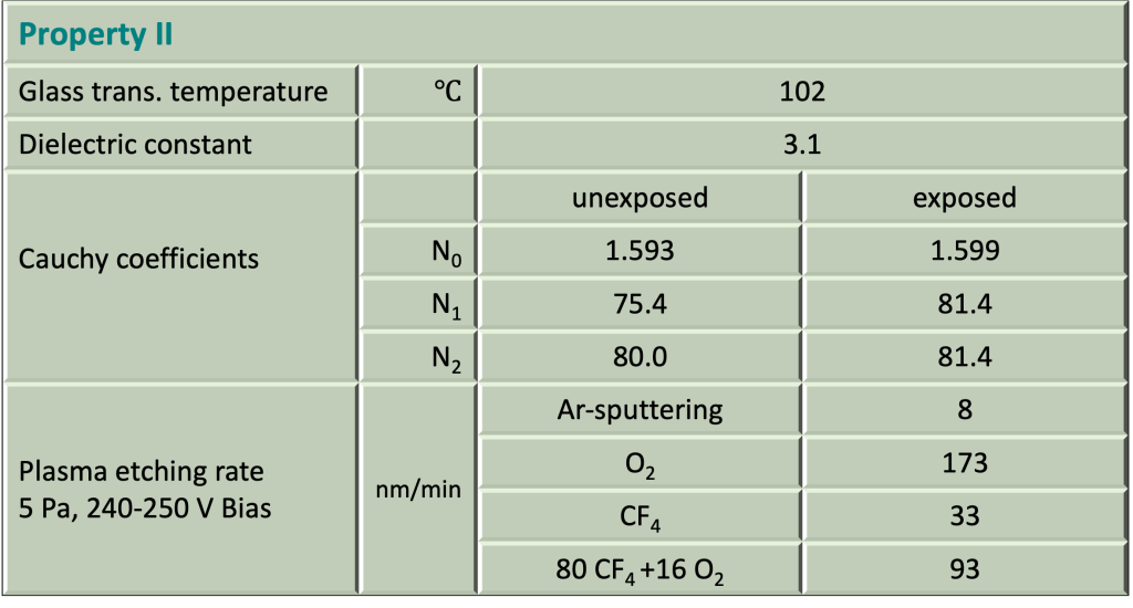
Product properties 產品物性

…
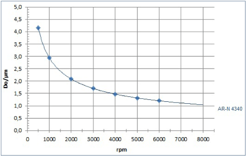
AR-N 4340 Spin curve 塗佈曲線
…
Structure and resolution 結構與解析度
Structure resolution
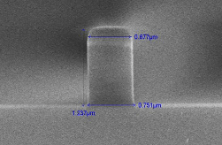
AR-N 4340 Film thickness 1.4 μm Resist structure 0.7 μm L/S
Resist structure
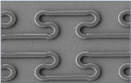
AR-N 4340 Film thickness 2.0 μm Resist structure 4.0 μm
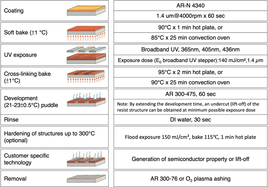
Process parameters
| Substrate | Si 4″ wafer |
| Soft bake | 85℃ x 60sec, hot plate |
| Exposure | i-line stepper (NA: 0.65) |
| Development | AR 300-475x60 sec, 22℃ |
Process chemicals
| Adhesion promoter | AR 300-80 |
| Developer | AR 300-475 |
| Thinner | AR 300-12 |
| Remover | AR 300-76 / AR 300-72 |
…
Process baseline 製程參數
This diagram shows exemplary process steps for AR-N 4340 photoresists. All specifications are guideline values which must be adapted to own specific conditions. For further information on processing, 👉“ Detailed instructions for optimum processing of photoresists”. For recommendations on wastewater treatment and general safety instructions, 👉”General product information on Allresist photoresists”.
表列為AR-N 4340 系列產品製程參數的範例。所有參數為參考值,使用者應依設備環境實際狀況加以調整。
…
Reference data for process tuning
TCD vs. bake temperature
| Temperature ℃ | TCD (s) | Dose (mJ/cm2) |
|---|---|---|
| 70 | 20 | 480 |
| 80 | 22 | 250 |
| 90 | 24 | 140 |
| 100 | 41 | 65 |
| 110 | 80 | 55 |
| 120 | 210 | 220 |
| 130 | ∞ | ∞ |
Development recommendations
| Resist | Developer | ||
| AR 300-26 | AR 300-26 | AR 300-475 | |
| AR-N 4340 | 1 : 1 | pure | pure |
Samples were dried at 85 °C and crosslinked at temperatures as indicated (developer: AR 300-475).The development strongly depends on the bake temperature.
Above a temperature of 130 °C, resist AR-N 4340 is not developable anymore. Optimum temperatures range between 90 and 100 °C.
樣品條件: 軟烤 85℃, 以表列溫度進行曝後考.顯影劑: AR 300-475顯影時間與曝後烤溫度有直接關係.曝後烤溫度達130℃, 光阻就無法被顯開.最適合曝後烤溫度介於90℃至100℃.
…
Linearity
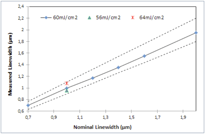
Up to a line width of 0.7 μm, the linearity is in the desired range. (parameter see graphic Focus variation)
Optimum exposure dose
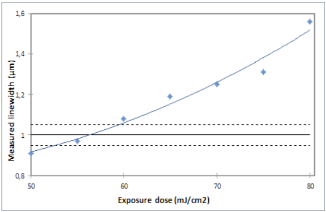
The optimum exposure dose for 1 μm-bars is 56 mJ/cm2.(parameter see grafic Focus variation)
…
Focus variation
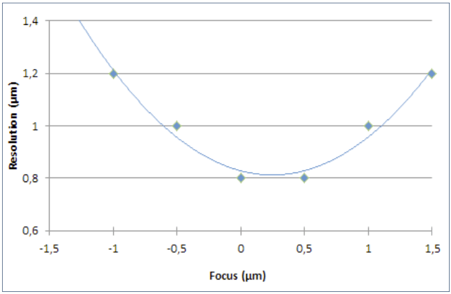
The resist achieves a resolution of 0.8 μm optimal focus adjustment REM measurement: Thickness 1,5 μm, PEB 105 °C, 180 s, l-line stepper (NA: 0,65), Developer AR 300-475.
Sensitivity in dependency on the bake
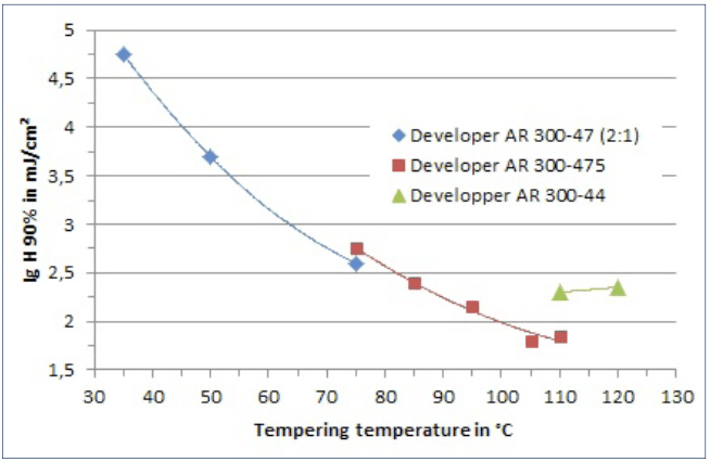
Samples were both dried and crosslinked at temperatures as indica- ted. The optimum working range is between 90 and 110 °C.
…
Time for complete development vs. bake
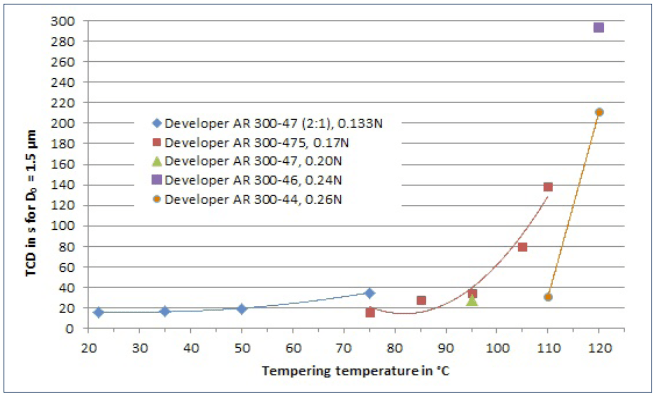
The time for complete development is very short at bake temperatures of < 50 °C, even if weak developers are used. With increasing temperature, the time for complete development (TCD) is considerably prolonged. Above a temperature of 120 °C, complete development of the resist is no longer possible.
Temperature stability after harding

Hardened resist bar structures after tempering at 200 °C
The developed structures are stable between 140 -160 °C, depending on the drying procedure (hot plate or oven). Structures can be stabilized up to temperatures of 220 °C by flood exposure and a subsequent bake at 120 °C.
…
