AR-P 6510 series thick EBL resist
high film thickness with e-beam lithography
…
Product brief 產品簡介
本產品膜厚可依需要調整,厚度範圍介於10 - 250um。產品曝光以電子束,同步幅射或X光,毋需於黃光室作業。屬電子束微影阻劑中,高膜厚應用.
…
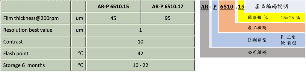
Product series & Code 產品比較及編碼說明:
…
Packing 產品包裝:
✅ 250 ml /瓶
✅ 1 L/瓶
其它包裝可依客戶需求增加.
Shipping 出貨:
本品未列於固定生產品項,價格交期需先詢問,
預估交期為
✅ 4 – 8 週. 徳國運出
…
Product Features 產品特性
- exposure with e-beam,synchrotron and x-ray (no yellow light required)
電子束,同步輻射或x光曝光,毋需於黃光室作業 - excellent image quality
微影品質優良 - solvent-based developer
使用溶劑型顯影劑 - film thickness values of 10 µm to 100 µm
目前版本膜厚為10 – 100 um. 調整配方可達250um
- process-stable
製程穩定 - solvent-based developer
使用溶劑型顯影劑 - high molecular weight poly(methyl methacrylate)
高分子成份為聚甲基丙烯酸甲酯(PMMA) - safer solvent PGMEA
使用較安全溶劑丙二醇甲醚醋酸酯
…
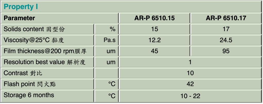
Product Properties 產品物性
…
Film thickness value 塗佈膜厚
| spin time 時間/speed轉速 | unit | Product/film thickness | ||
| 120 sec | 30 sec | AR-P 6510.15 | AR-P 6510.17 | |
| 200 rpm | 350 rpm | um | 45 | 95 |
| 350 rpm | 500 rpm | um | 28 | 56 |
These resists are designed for high film thicknesses which can only be obtained with low spin speeds. At spin numbers of < 1000 rpm, resists tend to form strings (candy floss effect). Thinner films can be realised if dilutions are used.
AR-P 6510主要使用於高膜厚應用,塗佈轉速不能太高。 當轉速低於1,000轉時容易產生絲狀物,(即所謂的棉花糖效應)。
稀釋產品,可獲得較低膜厚。
…
Structure resolution
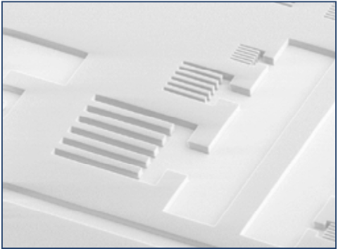
AR-P 6510.17 Film thickness 40 μm, structures up to 5 μm
Resist structures
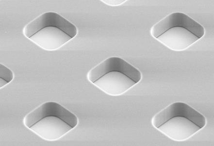
AR-P 6510.17 (diluted), exposure with e-beam (developer AR 600-55), film thickness 5 µm
…
Process baseline 製程參數
This diagram shows exemplary process steps for AR-P 6500 resists. All specifications are guideline values which have to be adapted to own specific conditions. For further information on processing, 👉“Detailed instructions for optimum processing of e-beam resists”. For recommendations on waste water treatment and general safety instructions, 👉”General product information on Allresist e-beam resists”.
表列為AR-P 6510.17阻劑產品製程參數的範例. 所有參數為參考值,使用者應依設備環境實際狀況加以調整
| AR-P 6510.17 | |
Coating | 45 um@350rpm x 5 min |
Soft bake (± 1℃) | 95℃ x 60 min hot plate. (temperature ramps recommended), or 90℃ x 3 hours, convection oven (temperature ramps recommended) |
e-Bean exposure | e-beam Exposure dose (E0): 5,000 μC/cm2 |
Development (21-23±0.5℃) puddle | AR 600-56, 15 min |
Development stop and rinse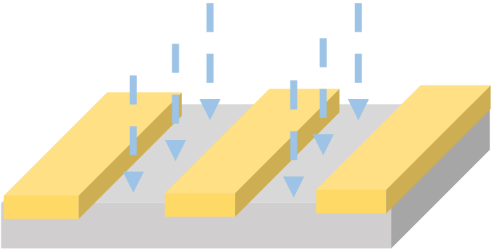 | AR 600-60, 30 sec / DI water, 30 sec |
Post-bake (optional)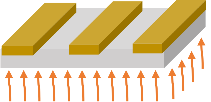 | 100℃ x 10 min hot plate, or 95℃ x 60 min convection oven for complete drying and slightly enhanced plasma etching resistance |
Customer specific technology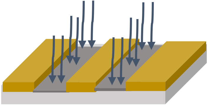 | LIGA application or the fabrication of x-ray masks |
Resist removal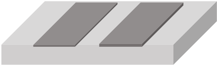 | AR 600-71, or O2 plasma ashing |
…
Processing instructions for coating
Prior to spin coating it is recommended to remove gases which may possibly be present. The highly viscous resist should therefore rest a few hours before use. A warming of resist bottles in a water bath to 50 °C max. to reduce the viscosity and the utilisation of ultrasound support the removal of gas bubbles. Resist deposition should be performed as carefully as possible to avoid any additional introduction of air bubbles. Slow spin speeds and low exposure times are advantageous (200 to 350 rpm, > 3 min). Edge bead formation can be reduced if the rotational speed is briefly increased towards the end of the coating procedure (for 10 s to max. 500 rpm). The amount of resist will also influence the film thickness; for 4 inch-wafers, the use of at least 10 g of resist are recommended. In order to obtain optimum film qualities, own experiments of each user are required.
建議塗佈之前先去除此高黏度阻劑中可能存在的氣泡:
-靜置數小時
-以不超過50℃溫水浴加熱瓶身以降低阻劑黏度
-輔以超音波處理以去除氣泡
-阻劑滴定時小心操作,以避免氣泡產生
建議以低轉數塗佈阻劑(200 – 350 rpm, >3 min)
塗佈程序最後段,建議短暫提高轉數(500rpm max. 10 sec)以降低阻劑在基板邊緣堆積隆起(edge beads)
滴定的阻劑數量也會影響厚度;以4寸晶元為例,建議滴定量為10g。
高黏度,高膜厚的阻劑,使用者的經驗與設備的良好搭配可獲得高品質膜厚。
…
