High-resolution negative e-beam resist AR-N 7520.17new for etching application
At the institute FEMTO-ST in France, very even and smooth 300nm ridges could be achieved with AR- 7520.17new and a coating thickness of 400nm . In the following etching application, the resist geometry could be transferred into the Si substrate in excellent quality. Due to the good etch resistance in the plasma used (ICP, SF6:C4F8), a selectivity of 12:1 could be achieved.
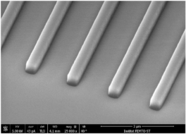
AR-N 7520.17, parallel 300 nm lines, film thickness 400nm, SB 1′ @ 85°C, Raith eLine, 30 kV, dosage 120 µC/cm², devlopment 2′ AR 300-44 (0.26n TMAH), cleaning with oxygen plasma
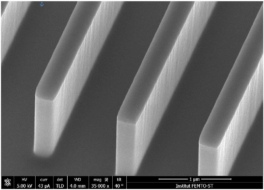
ICP etched architecture, mixture SF6:C4F8 / 400 W / Selectivity 12:1, stripping with oxygen plasma
Overview of photoresist FAQs
AR-N 7700-4um thick-proximity effect
Chemically amplified, highly sensitive negative e-beam resist SX AR-N 7730/37
Diffractive optics with the “analogous“ e-beam resist
High-resolution negative e-beam resist
High-resolution negative e-beam resist AR-N 7520.17new for etching application
Medusa 82 for EUV applications
Medusa 82 with photoacid generator (PAG)
Medusa 82 – the alternative to HSQ-resists, storage stability
Medusa 82: Influence of post exposure bake (PEB)
Ratio resolution and dose, exemplarily shown for e-beam resist SX AR-N 7530/1)
Sensitive, etch-stable negative e-beam resist for processes without yellow light
