AR-N 7700, 4 µm thick, proximity effect
The general aim of electron beam lithography is to achieve a maximum resolution, and therefore mostly very thin layers are used (50 – 500 nm). In a few cases however also very small structures with high aspect ratio are of interest. Examples for possible applications are electroforming processes or the generation of a nano-library for the storage of smallest substance samples. For this purpose, 4 μm-thick layers of the e-beam resist SX AR-N 7700.38 were exposed, tempered and developed (AR 300-47).
The acceleration voltage was 20 kV, the current 50 pA. Structural width values were strongly dose-dependent. In the case of an overexposure, the proximity effect (which is particularly pronounced at an acceleration voltage of 20 kV) becomes clearly visible as evident from the broadening of structures (Fig. 2).

Fig. 1 Bars: 500 nm, height: 4 μ m, 30 μ C/cm², 20 kV
If an optimal dose is applied, 500-nm bars can be generated with a film thickness of 4 μm (aspect ratio 8). The aspect ratio is expected to improve further at higher acceleration voltages.
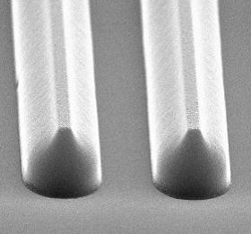
Fig. 2 Bars: 1 μ m, height: 4 μ m, 50 μ C/cm², 20 kV
Overview of photoresist FAQs
AR-N 7700-4um thick-proximity effect
Chemically amplified, highly sensitive negative e-beam resist SX AR-N 7730/37
Diffractive optics with the “analogous“ e-beam resist
High-resolution negative e-beam resist
High-resolution negative e-beam resist AR-N 7520.17new for etching application
Medusa 82 for EUV applications
Medusa 82 with photoacid generator (PAG)
Medusa 82 – the alternative to HSQ-resists, storage stability
Medusa 82: Influence of post exposure bake (PEB)
Ratio resolution and dose, exemplarily shown for e-beam resist SX AR-N 7530/1)
Sensitive, etch-stable negative e-beam resist for processes without yellow light
