PPA polymer, preparation kits and AR-P 8100
Base polymer for thermal scanning probe lithography (tSPL) resist
…
PPA polymer Product brief 產品簡介
聚苯二甲酸 (PPA Polyphthalaldehyde)為白色粉末狀高分子,配製成溶液(例如AR-P 8100)應用於熱掃描微影(tSPL-Thermal Scanning Probe Lithography)阻劑,可獲的高解析度的結構(10nm)。ㄧ般以溶劑(AR 600-02 anisole 甲氧苯)配製成需要的溶液濃度塗佈於基板上。產品的包裝,出貨,配製與應用說明如後:
…
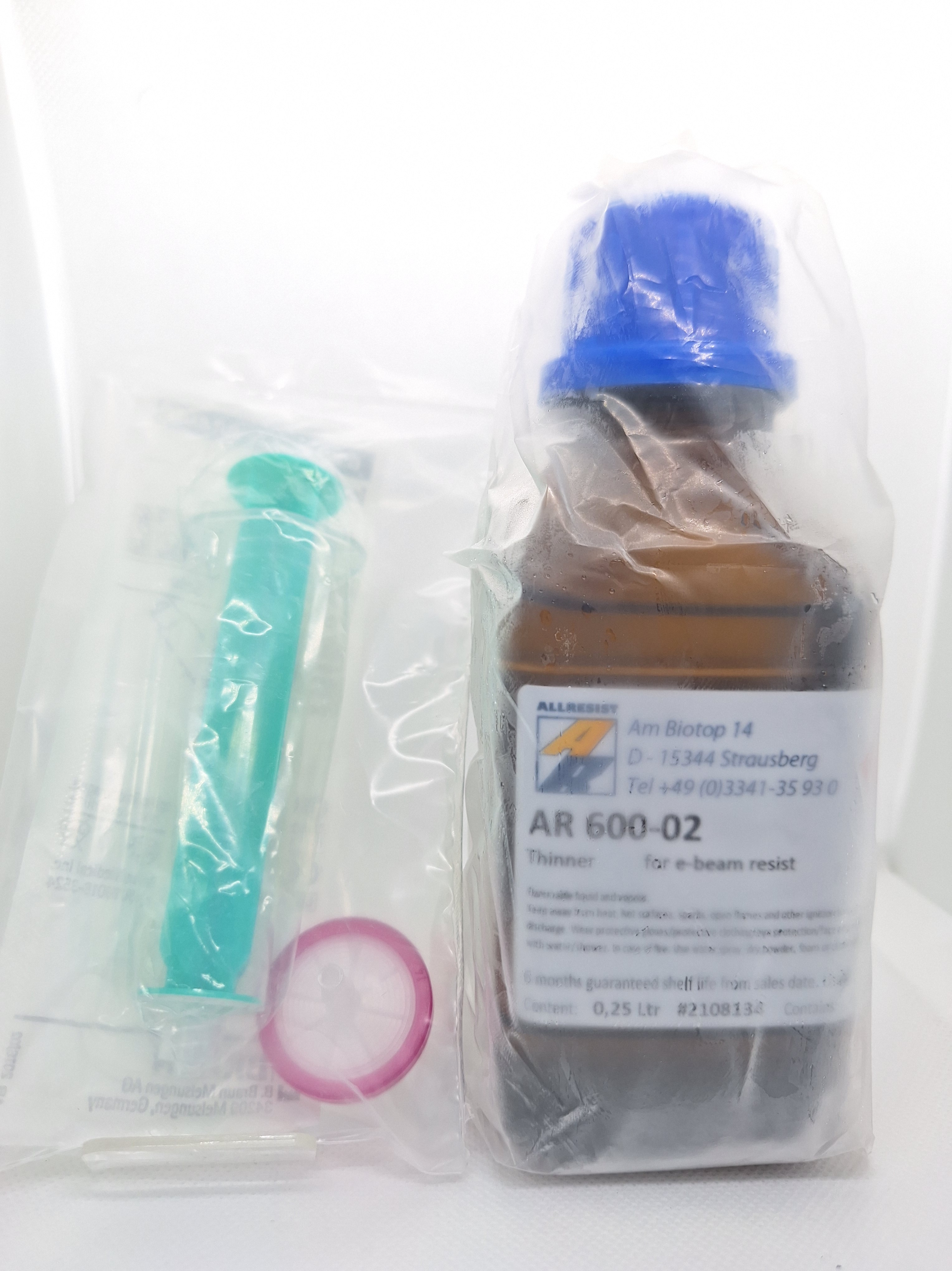
Packing 產品包裝:
✅ 1 g/瓶
✅ 1 set
包含:
1g PPA
AR 600-02 250ml
針筒
過濾器 0.2um PTFE
其它包裝可依客戶需求增加.
Shipping 出貨:
✅ 2 – 4 週: 徳國運出
❎ 1 週: 國內庫存
(目前暫無國內庫存)
PPA set
…
Information on PPA, the base polymer of Phoenix 81
Anionically polymerized polyphalaldehyde (PPA), the base polymer for the thermo-structurable resist Phoenix 81, is a white powder which is storage-stable for at least 4 weeks at room temperature. PPA can thus be shipped with standard shipping and does not require the highly cost-intensive refrigerated transport of PPA solutions.
When stored in a refrigerator (8 – 12 °C), the PPA polymer is stable for at least 6 months. For long-term-storage, we recommend temperatures of -18 °C since this ensures that PPA remains stable for at least one year.
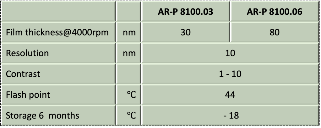
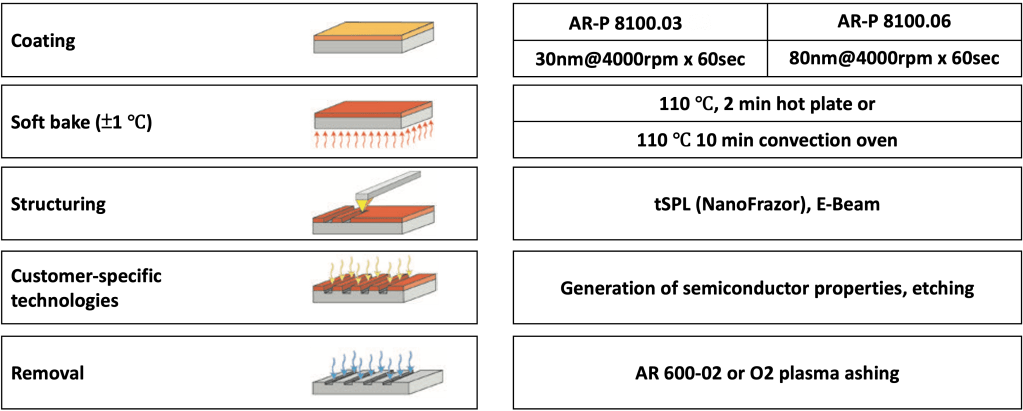
The polymer PPA dissolves easily in anisole. By varying the polymer concentration, solutions can be produced flexibly to realize different film thicknesses values. The film thicknesses can furthermore be varied by changing the spin speeds. This is exemplarily shown for AR-P 8100.03 (solids content: 2.5 %) and AR-P 8100.06 (solids content: 5.5%) in the table “Properties I“.
聚苯二甲酸由苯二甲醛經陰離子聚合法聚合而成,為白色粉末狀。可做為熱掃描微影的基礎成份,例如調配成Phoenix 81 (AR-P 8100)可立即使用的阻劑(ready-to-use tSPL resist)。
PPA polymer在室溫下可維持穩定約4週的時間,可以常溫運輸而無需像配製好的溶液需以昂貴的低溫運輸(-18℃)。
PPA polymer的儲存建議為:
8 – 12 ℃ – 可維持穩定至6個月
-18℃ – 可維持穩定至少1年。長期存放建議以此溫度。
PPA polymer可於甲氧苯溶解。以其為溶劑可依需要的厚度調配溶液濃度。厚度範圍可以塗佈轉速進一步微調。
範例可參考第四頁AR-P 8100.03 (固型份 2.5%)及AR-P 8100.06 (固型份 5.5%)的物性表.
…
PPA溶液濃度與塗佈厚度對應曲線
The following graph shows the relationship between polymer concentration and resulting film thickness
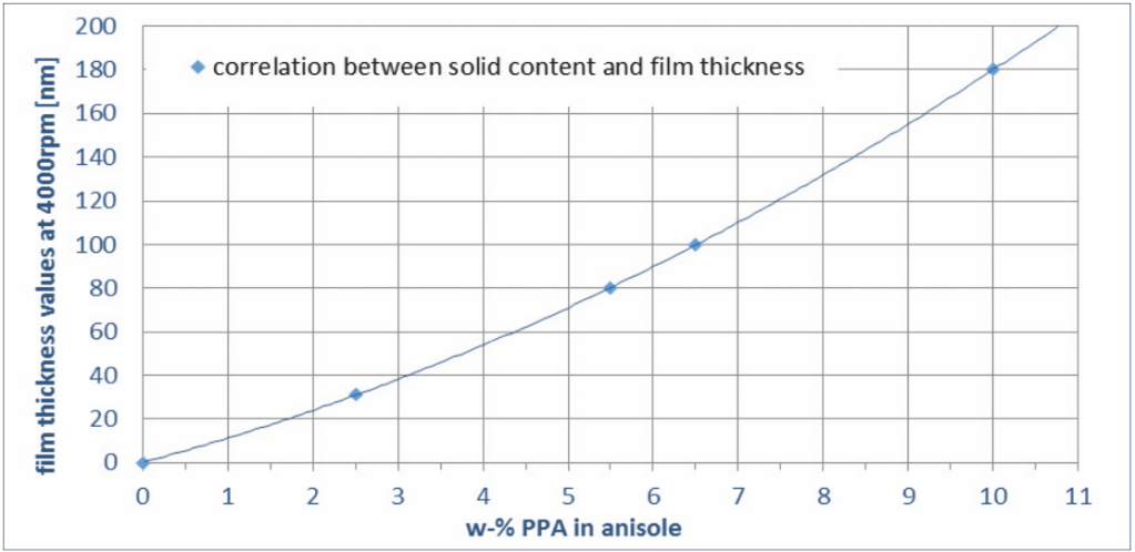
Dependency of film thickness on solids content (anionic PPA in anisole, 4000 rpm, 30 s, open chuck)
…
Preparation and use of PPA solutions溶液配製與應用
- To prepare the PPA solutions, the weighed quantity of PPA is given into a suitable vial before the calculated amount of anisole is added. The mixture is stirred or shaken at room temperature until after about 10 minutes a clear, homogeneous solution results.
先將秤重後的PPA置入適當玻璃瓶後再加入計量的甲氧苯溶液。於室溫下攪伴或搖晃混合物約10分鐘至混合成微清徹均勻的溶液。 - The PPA solution is transferred into a syringe of appropriate size and filtered using a 0.2 μm syringe filter into a dry and clean bottle.
將溶液置入類似容量針筒並以規格0.2um過濾至乾淨瓶裝容器
Formulation example for 2.5 % solution 配製2.5%溶液範例
2.5 g PPA + 97.5 g anisole = 100.0 g of 2.5 % 0.2 μm filtrated polymer solution. This corresponds to AR-P 8100.03 with respect to the properties. Please note: 2.5 % is rounded up to 3 % in the product designation.
2.5克 PPA + 97.5克的甲氧苯=100克的2.5%過濾溶液。過濾規格為0.2um。此為與AR-P 8100.03類似特性的溶液。附註: 3%為2.5%四捨五入後的值。
Storge 儲存
PPA solutions are only stable at low temperatures; we thus recommend storage at -18 °C. In this case, solutions are stable for at least 6 months. Prior to use, solution should be warmed to room temperature to avoid condensation of moisture. Short-term use of PPA solutions at room temperature (up to 3 hours) will still ensure the high product quality.
配製好的溶液建議儲存於零下18度的溫度(-18℃)。溶液於此溫度可維持穩定約6個月
使用前需回溫以避免濕氣凝結。
為維持品值穩定,溶液於室溫下建議於3小時之內使用完畢。
…
PPA solution-AR-P 8100 brief 原廠配製溶液說明
AR-P 8100為原廠配製好的即用型(ready-to-use)熱掃描微影阻劑。優點是無需自行調配。缺點是需在低溫-18℃下運輸,成本較高。在此低溫下儲存,有效期約6個月。目前配製的濃度有:
AR-P 8100.03
AR-P 8100.06
Product series & Code 產品比較及編碼說明:
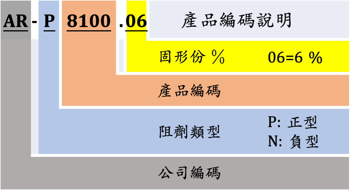
註:6%為5.5%的四捨五入
…
Packing 產品包裝:
✅ 250 ml/瓶 (需待批次生產)
✅ 1 L/瓶 (需待批次生產)
其它包裝可依客戶需求增加.
Shipping 出貨:
本品運輸需低溫(-18℃),未列於固定生產品項,價格交期需先詢問,建議評估PPA polymer自行調配。
如需向原廠選購配製液,預估交期為
✅ 4 – 8 週: 徳國運出
…
PPA solution AR-P 8100 Features 產品特性
- for tSPL (thermal Scanning Probe Lithography)
熱掃描微影專用阻劑 - film thickness 20 – 160 nm
膜厚範圍:20 – 160 nm - high resolution (< 10 nm) and very high contrast
高解析度(< 10nm),高對比 - very process-stable
製程穩定
- not photosensitive > 300 nm
對波長>300nm不感光 - well suited for two-layer processes (lift-off) and “overlay pattern”
適合懸浮剝離的雙層製程及疊覆結構 - application in grey-tone & e-beam lithography
灰階製程及電子束微影 - solution of PPA in safer solvent anisole
PPA溶於較安全甲氧苯溶劑
…
PPA solution Properties 產品物性
…
PPA solution spin curve 塗佈曲線

…
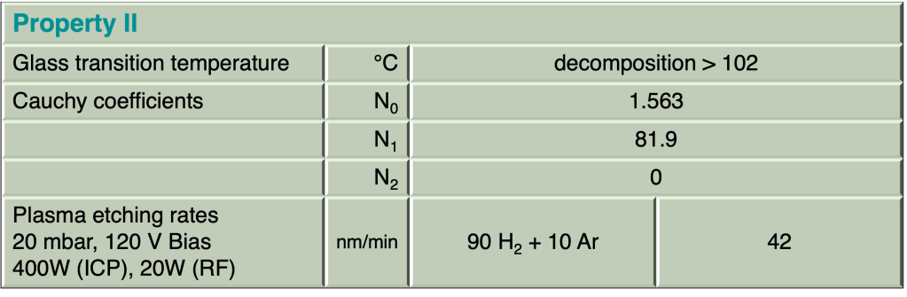
Structure of grey-tone interferenz
Etched sinus pattern
Resist structures
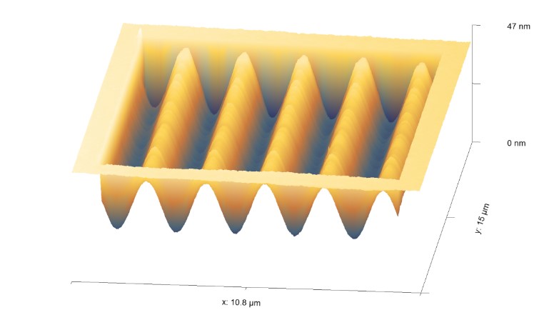
Plasmonic trimer of 30 nm gold discs with 20 nm distance
Process parameters
| Substrate | Si wafer |
| Soft bake | 110℃x2min, hot plate |
| Structuring | NanoFrazor |
Process chemicals
| Adhesion promoter | AR 300-80 new/HMDS |
| Thinner | AR 600-02 |
| Remover | AR 600-01 / AR 600-02 |
…
Process baseline 製程參數
This diagram shows exemplary process steps for AR-P 8100 series resists. All specifications are guideline values which have to be adapted to own specific conditions. For further information on processing, 👉“Detailed instructions for optimum processing of e-beam resists”. For recommendations on waste water treatment and general safety instructions,
👉”General product information on Allresist e-beam resists”.
表列為AR-P 8100系列產品製程參數的範例. 所有參數為參考值,使用者應依設備環境實際狀況加以調整
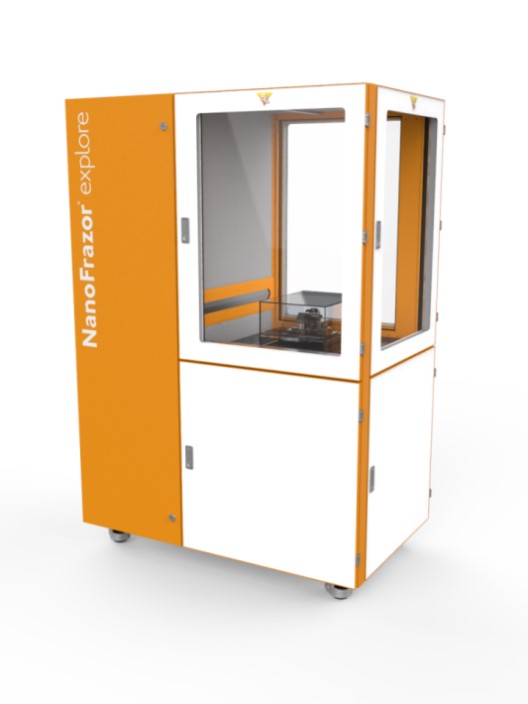
NanoFrazor technology
Polyphthalaldehydes (PPA) are thermally structurable resists which were mainly developed for tSPL applications with the NanoFrazor (SwissLitho AG). Key element of this device is a hot needle scanning the resist surface. With each tip, the thermally sensitive PPA evaporates, thereby transferring the desired structures into the layer. Both 10 nm-lines as well as sophisticated three-dimensional structures can be written in this way.
The NanoFrazor technology allows writing structures without vacuum conditions. Due to the specific technology, it is also possible to set up the device in a clean laboratory. A cleanroom is required for the coating the substrates with resist Phoenix 81. The write speed of the NanoFrazor is comparable to the speed of simple electron beam devices for the realization of high-resolution structures.
聚苯二甲酸為熱掃描微影技術主要使用的高分子。設備有SwissLitho公司的NanoFrazor。核心技術為熱探針元件掃描阻劑,探針頭的熱源使PPA阻劑蒸發而寫出需要的圖案。運用此技術可寫出10nm線及精密的立體結構。NanoFrazor設備無需真空環境,因此在乾淨的實驗室即可設置。只需要無塵室以塗佈其專用阻劑AR-P 8100。在高解析度的結構,熱掃描速度約與電子束微影相當。
Processing recommendations
Phoenix 81 is not storage-stable at room temperature and should thus be kept cooled at -18 °C. To ensure our high-quality demands, this product is only shipped in powder form as PPA polymer á 1g.
Prior to coating, the PPA solution should be adjusted to room temperature. Brief heating has no significant influence on the stability. PPA layers are thermally sensitive, but significant decomposition processes are only observed above temperatures of 120 °C.
AR-P 8100(或由PPA配製好的溶液)在室溫下並不穩定,最好存放於零下18度(-18℃)的低溫。為確保品值,本產品僅以PPA高分子形態運輸。
進行塗佈前,從低溫取出的PPA溶液(AR-P 8100)需進行回溫。回溫時稍微加熱不會影響穩定性。
PPA塗層對溫度敏感,但溫度需超過120℃才會分解。
…
Two-layer process 雙層製程參數
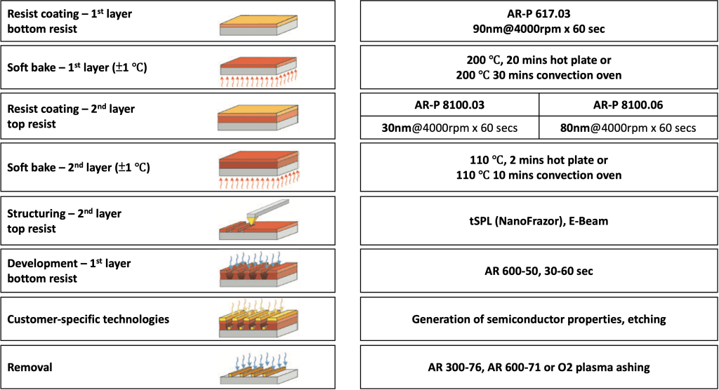
Additional information concerning positive two-layer systems 雙層阻劑懸浮剝離製程說明
Coating塗佈
At first, AR-P 617.03 is coated and tempered. After cooling to room temperature, Phoenix 81 is applied as top resist. The layer thickness can be varied in a range between 20 nm and 160 nm. Subsequently, the two-layer system is tempered. The thickness ratio of both layers influences the structural geometry. To obtain a strong lift-off effect, a thin PPA layer and a thick bottom layer is recommended. For a dimensionally accurate pattern transfer however, both layers should be approximately equal in thickness. The entire system must be optimized regarding the respective application.
雙層製程的塗佈,先塗佈AR-P 617.03並進行軟考。待冷卻至室溫再進行PPA層塗佈(AR-P 8100)。厚度範圍為20nm至160nm。接著再對雙層阻劑進行軟考。
兩層厚度的比例會影響製程,厚的第一層(AR-P 617.03)加上較薄的PPA層會有較佳的懸浮剝離效果(lift-off). 如果要有較佳的轉寫效果,則兩層厚度需控制一樣。因此需依應用控制圖佈厚度。
Development顯影
Development of the lower layer exclusively takes place in those areas which were exposed by the NanoFrazor. PPA layers are not attacked by developer AR 600-50. The development is isotropic and proceeds with defined speed. Both the duration of the development and the developer temperature strongly influence the extent of the undercut. The longer the developer exerts its in- fluence and the higher the developer temperature, the more pronounced is the undercut obtained.
上層的PPA層被熱掃描(NanoFrazoe)打開後才會對第一層阻劑顯影。PPA層不會被顯影劑AR 600-50攻擊。
顯影是等向性的並以設定的速度進行。顯影時間與溫度均會影響下切結構。顯影溫度越高越有下切效果,顯影時間越長越強化下切效果。
Lift off / Removing 懸浮剝離與去除
Suitable for the final lifting are remover AR 300-76 or AR 600-71.
AR 300-76或AR 600-71適合用來最後的剝離去除。
…
Application examples各種曝光法應用實例
…
Patterning of PPA with e-beam lithographyPPA以電子束微影
PPA layers can also be positively patterned directly by electron irradiation. Similar to the irradiation of commonly used e-beam resists like CSAR 62 or PMMA, electron beam exposure induces fragmentation of the polymer chains.
Polymer fragments resulting from PPA are however unstable and decompose into the volatile ortho-phthalaldehyde. Only very small amounts of monomeric phthalaldehyde are directly released in the device during e-beam exposure; only the subsequent PEB leads to an almost complete thermal development. But even in the range of the dose to clear (approx. 30 – 40 μC/cm2), a resist layer with a thickness of a few nanometers will remain. A residue-free substrate surface can nevertheless be obtained if a short plasma etching step is added.
The gradation passes through a minimum, but with increasing dose, also the concurrent cross-linking processes become increasingly important. This undesirable side reaction is due to radicals which are generated during electron irradiation and stabilize the layer by cross-linking. These effects also occur in PMMA layers, but only at much higher exposure doses, and are here used to produce negative PMMA architectures.
To determine the resolution limits of AR-P 8100, line patterns were examined in detail at the company Raith. Lines of different width were written into the PPA layer. After PEB and subsequent platinum metallization, metal bridges of < 20 nm width were obtained. The highest resolution that could be achieved was 16 nm.
與電子束微影阻劑,例如CSAR 62或是PMMA類似,PPA阻劑的塗層也可直接以電子束曝光。電子束能量會使高分子斷鏈而解離。解離的碎片不穩定而進一步分解成揮發性的鄰苯二甲醛。在電子束曝光下僅有少量的苯二甲醛單體會釋出,後續的曝後烤(PEB)會使其完全分解(熱顯影)。
但是,就算在安全劑量範圍(約30-40uC/cm2),阻劑層仍會殘留幾奈米的厚度。短時間的電漿蝕刻可清除殘留。
電子束曝光的另一副作用則是存在的自由基產生的架橋反應會影響解析度。類似於PMMA阻劑於高劑量電子束曝光時變成負型阻劑的製程。
為測試PPA解析度能力,Raith公司寫入不同線寬的PPA層,曝後烤後接著沉積白金。可獲得<20nm的線寬。實驗的最佳解析度可達16nm。
Lines written in PPA (resist AR-P 8100)
bridge with width of 16 nm, obtained after sputter coating with platinum (film thickness: 4 nm)
Adding PAGs (photo acid generator) to PPA (sample SX AR-P 8100/5) can increase the sensitivity and allow a better control of the gradation. The exposure causes a release of acid in situ which decomposes the PPA layer at 95 – 100 °C during the following PEB (positive development). The thermally induced, solvent-free development proceeds almost completely. Despite the addition of PAGs, a very thin residual resist layer however remains.
If PAG-containing resists are used together with AR-P 617 in two-layer process, the thin remaining resist layer will not disturb the further process sequence since it is dissolved during the subsequent development. After e-beam exposure and PEB, bottom resist AR-P 617 is selectively developed with developer AR 600-50. The undercut is adjusted specifically by varying the duration of the development step. Reliably processable lift-off resist architectures can thus be produced. This method allows the realization of metal bridges (platinum):
The process window is however quite narrow; already small variations of the dose affect the obtained line width considerably.
實驗樣品(SX AR-P 8100/5)是在PPA溶液中添加光酸產生劑(PAG),以增加其敏感度可有較好的階度控制。機制是曝光時產生的光酸促使PPA層在隨後的95 – 100℃曝後烤時分解。這種無溶劑的熱顯影方式還是會有極薄的殘留層。(左下圖階度曲線)。
如果與AR-P 617應用於雙層製程則無殘留層問題。殘留層會在AR-P 617電子束曝光,曝後烤及以AR 600-50顯影時完全溶解。下切結構可以顯影時間控制。右下圖白金金屬橋結構為範例。只是製程寬容度不高,曝光劑量稍為變動就會影響線寬。
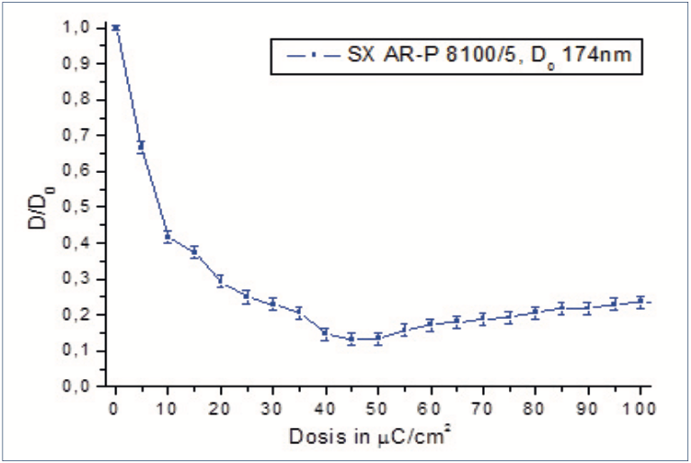
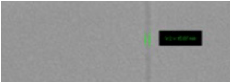
Gradation of SX AR-P 8100/5 after PEB at 98 °C
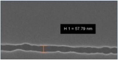
Platinum bridges width:58nm
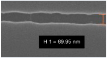
Platinum bridges width:70nm
…
Patterning of PPA with photolithographyPPA以UV波長曝光
PPA layers can also be structured directly by means of photolithography. Irradiation with UV-light of a wavelength of < 300 nm results in a cleavage of the polymer chains to form volatile components.
By adding PAGs (photo acid generators), the photosensitivity can be significantly increased. The exposure releases acid in situ which then decomposes the PPA layer at 95 – 100 °C during the subsequent PEB (positive development).
The thermally induced, solvent-free development step proceeds almost completely. Cross-linking processes which are also induced by UV-exposure may however cause a thin, only a few nanometres thick residual resist layer. A residue-free substrate surface is obtained after addition of a short plasma etching step.
PPA層亦可以波<300nm的紫外線曝光,此波段會導致PPA斷鏈而形成揮發成份。
PPA溶液中加入光酸產生劑(PAG)會明顯的增加感光性。曝光產生的光酸會促使PPA層在95 – 100℃的曝後烤中分解。此為無溶劑熱顯影製程。
在曝光中,亦有可能產生架橋反應形成幾奈米厚的殘留,以電漿蝕刻可去除殘留層。
…
Structuring with laser (pulse)PPA以雷射直寫
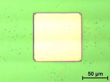
PPA layers can also be structured by laser ablation. Substrates coated with AR-P 8100 were patterned at the IOM Leipzig with pulsed laser light at different wavelengths. This enabled the realization of architectures with very low edge roughness. In the absorption range of PPA (at 248 nm), complete ablation was achieved without damage of the silicon substrate.
PPA層亦可以雷射直寫。在德國的萊布尼茲表面工程研究所以不同波長的脈衝雷射直寫塗佈AR-P 8100的基板,驗證雷射直寫的圖案邊緣粗燥度低。下圖為以248nm直寫的圖案
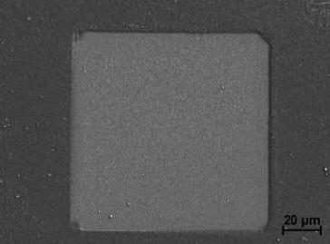
Even though PPA shows only a very low absorption at a wavelength of 355 nm, a selective ablation with comparatively high sensitivity is nevertheless possible. The structures realised here are again characterized by very smooth edges.
PPA層對波長355nm的吸收較低,選擇性的直寫仍可有不錯的敏感度。如下圖範例仍可獲得平滑的邊緣。
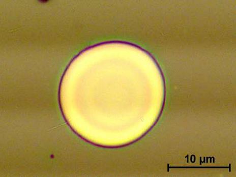
0.1 J/cm2, 355 nm ps-laser, single-pulse exposure, 700 nm PPA on Si-wafer
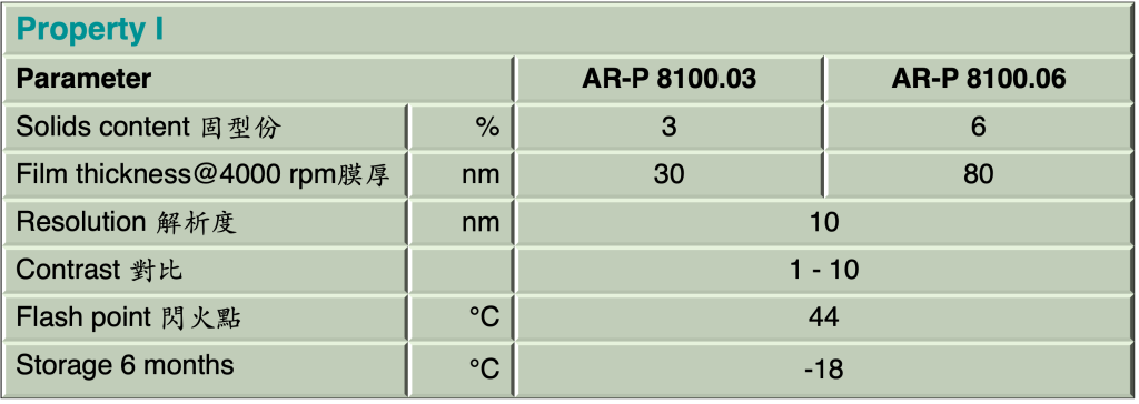
The laser beam can also be used to generate 3D structures. Interference projection through a phase mask allows the production of lattice structures with sinusoidal shape and very low surface roughness..
透過干涉投影及相轉移光罩的機構,雷射直寫可以用來產生立體結構。下圖為說明及鎖產生的格子圖案。
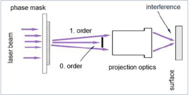
Experimental setup of interference projection


SEM-image of PPA lattice with sinusoidal progression (period ~750 nm);
248 nm, 20 ns pulses, number of pulses: 10; 700 nm PPA on Si-wafer
…
