AR-P 3740 standard positive i-line photoresist
Sensitive photoresist for sub-um semiconductor devices
…
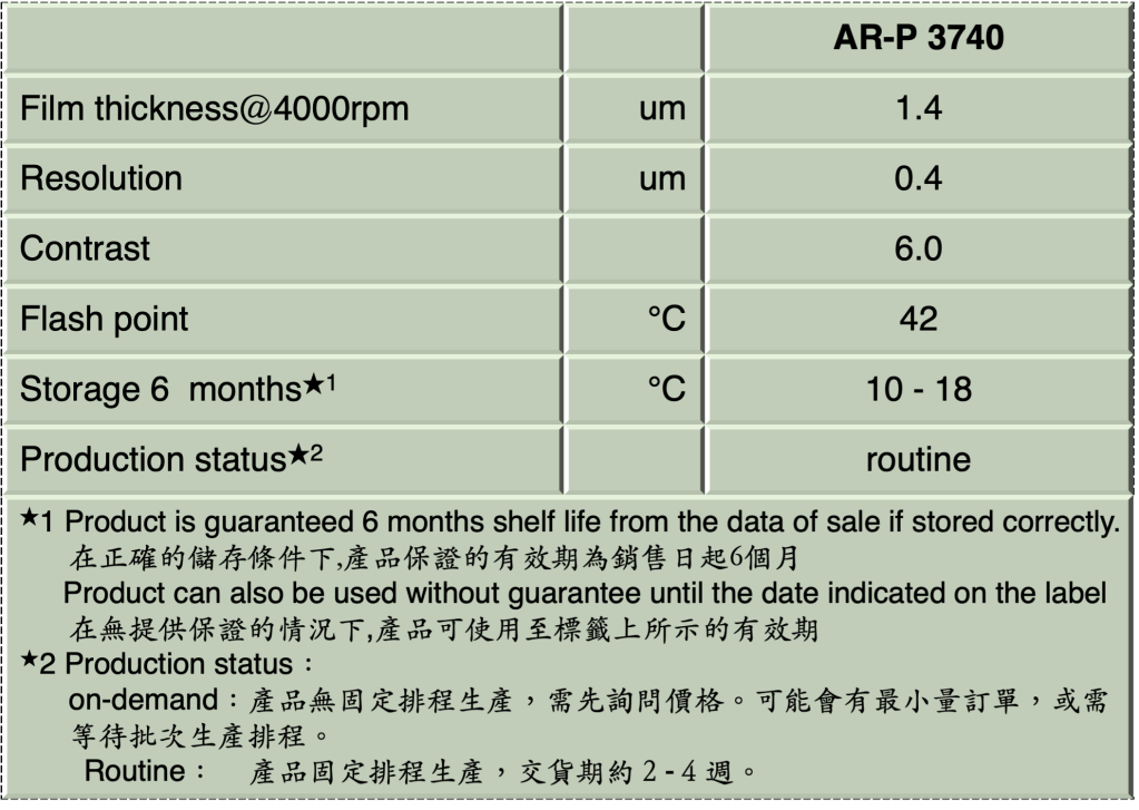
AR-P 3740 product brief 產品說明
AR-P 3500 產品為高敏感度正型i-line光阻,適合次微米高密度積體電路製程。
產品基本資料如下:
…
Packing & shipping 產品包裝與出貨
packing 產品包裝
✅ 250 ml/瓶
✅ 1 L/瓶
其它包裝可依需求研擬增加
shipping 產品出貨
✅ 2 – 4 週。德國運出。
❎ 1 週。國內庫存。
(目前暫無國內庫存)
…
Product features 產品特性
- broadband UV, i-line, g-line
曝光波長: 寬頻紫外線, i-line (365nm) , g-line (436nm) - high sensitivity, highest resolution up to 0.4 µm
高敏感度,最高解析度可達0.4 um - high contrast, excellent dimensional accuracy
高對比,尺寸精確度良好 - optimized coating properties on topologically complex substrate surfaces
塗佈特性適合基板表面複雜的高低結構 - plasma etching resistant, stable up to 120 °C
耐電漿蝕刻,耐溫可達120℃ - colored resist to prevent the effect of standing waves e.g. AR-P 3840
阻劑參雜染料可預防駐波效應(例如產品AR-P 3840) - combination of novolac and naphthoquinone diazide
主要成份為酚醛樹酯及叠氮基萘醌 - safer solvent PGMEA
使用較安全溶劑丙二醇甲醚醋酸酯
…
Product properties 產品物性

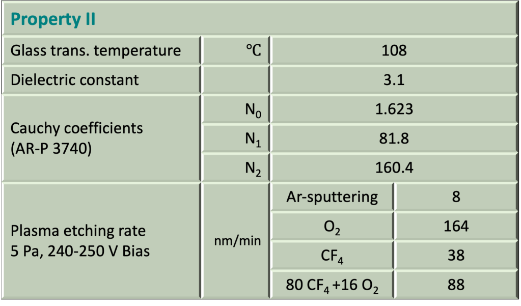
…
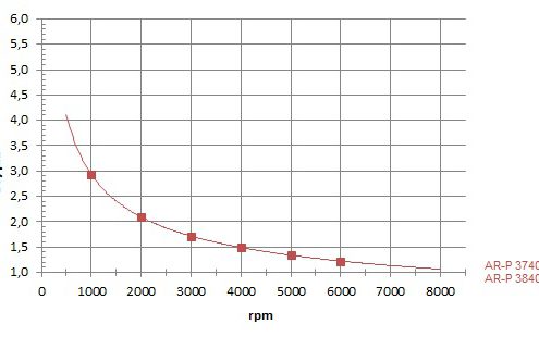
AR-P 3500 series Spin curve 塗佈曲線
…
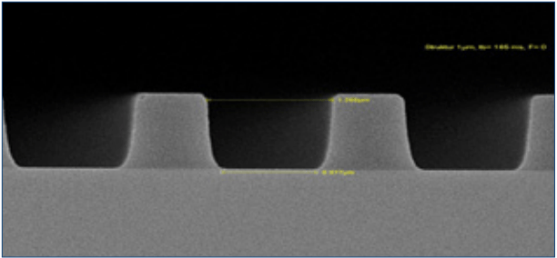
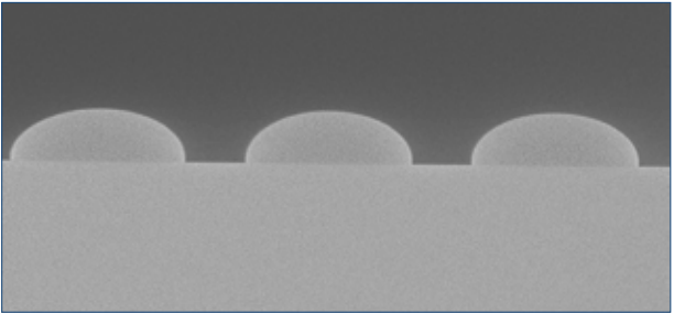
Structure and resolution 結構與解析度
Structure resolution
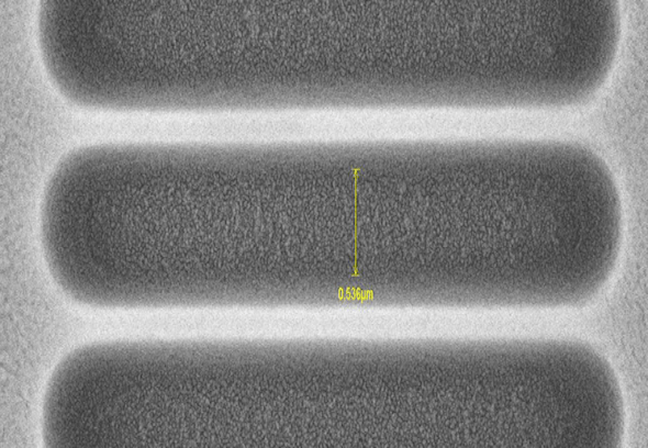
AR-P 3740
Film thickness 1.1 µm Resist structures 0.5 µm L/S
Resist structure
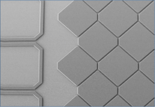
AR-P 3740
Film thickness 1.8 µm Resist structures up to 1.0 µm
…
Process baseline 製程參數
This diagram shows exemplary process steps for AR-P 3740 resists. All specifications are guideline values which must be adapted to own specific conditions. For further information on processing, 👉“ Detailed instructions for optimum processing of photoresists”. For recommendations on wastewater treatment and general safety instructions, 👉”General product information on Allresist photoresists”.
表列為AR-P 3740產品製程參數的範例。所有參數為參考值,使用者應依設備環境實際狀況加以調整。
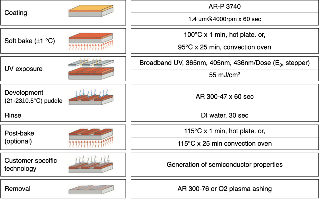
Development recipe
…
Reference data 參考資料
Dark erosion
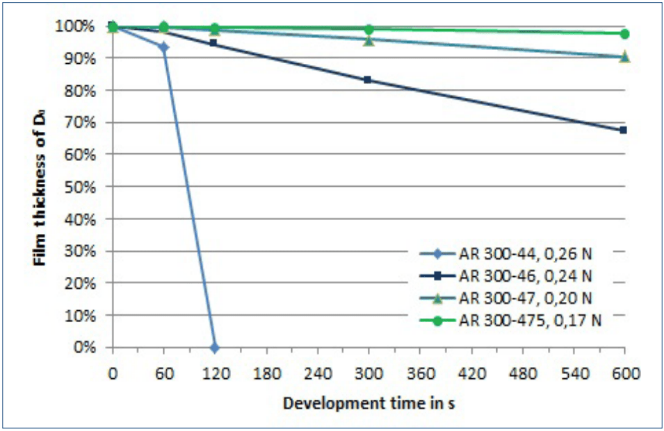
AR-P 3740 may be developed with any of the four TMAH developers. A high sensitivity is associated with high erosion rates. No dark erosion is obtained if weaker developers are chosen (see diagram Influence of developer strength)
Dark erosion
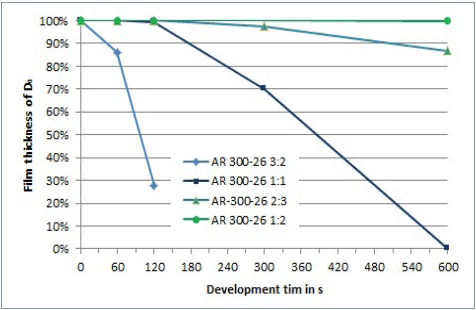
Using a dilution series of AR 300-26, the desired development properties can be adjusted accordingly. A dilution of 3:2 (3 parts AR 300-26, 2 parts DI water) is not recommended, due to the high erosion rate. More suitable in this case is a dilution of 1:1 to 2:1.
Influence of developer strength of the dark erosion
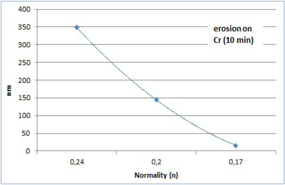
Using coated Cr-substrates (thickness 1.5µm), 15–350 nm are removed within 10 min depending on the respective developer strength. The highest erosion is obtained with the strong developer AR300-46 (0.24 n).
Influence of developer strength of exposure dose
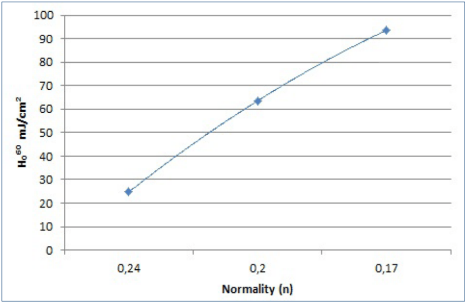
Using the strong developer AR 300-46, short exposure times can be realized. The highest contrast and thus a slightly higher resolution is obtained with the weak developer AR 300-475 (0.17 n).
Dependency of sensitivity (exposure dose) on resist drying
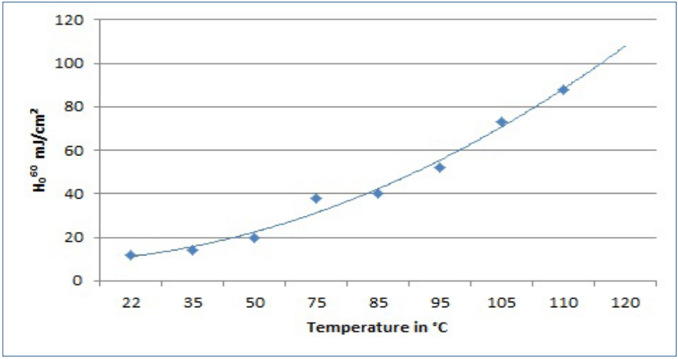
| Temperature ℃ | time | H060 mJ/cm2 | |
|---|---|---|---|
| Room | 22 | 24 h | 12 |
| convection oven | 35 | 4 h | 14 |
| 50 | 1 h | 20 | |
| 75 | 30 min | 38 | |
| 85 | 40 | ||
| 95 | 52 | ||
| 105 | 73 | ||
| 110 | 83 | ||
| 120 | — |
Performed by broadband UV with developer 300-35 1 : 1
It is also possible to develop resists which were only dried at room temperature (24 h). In this case, resists are technically very sensitive, but are however also characterized by high dark erosion. A good development is provided for resists baked at up to 110 °C (AR 300-35, 1 : 1), while developers with higher strength are required for bake temperatures above 120 °C (AR 300-35, 2 : 1). Resist layers tempered at 130 °C are basically non-developable any more.
Linearity
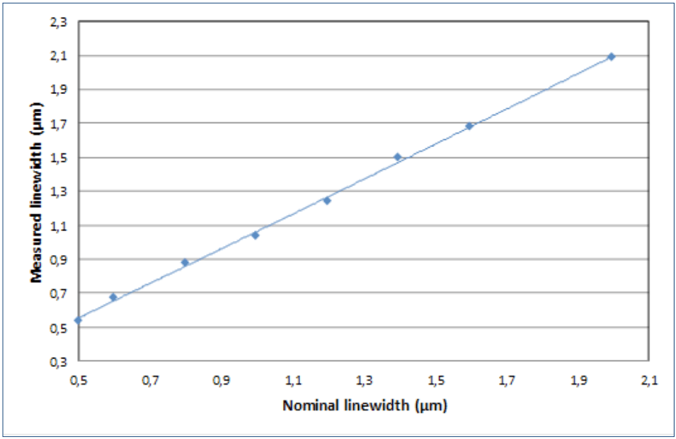
Up to a structure width of 0.5, a very good agreement is obtained.
Optimum exposure dose
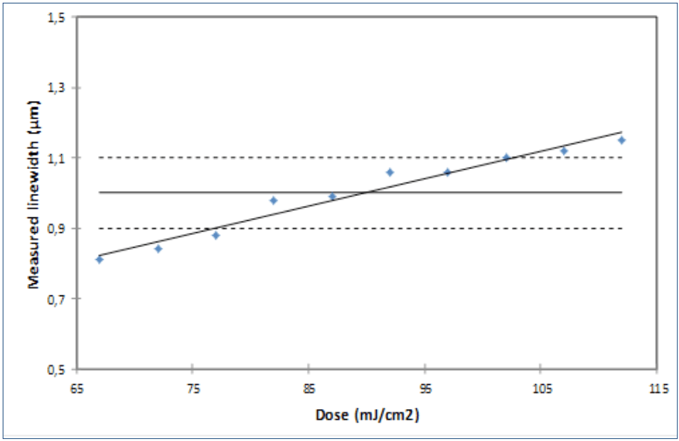
The optimum exposure dose for 1 µm lines is 88 mJ/cm2
Focus variation
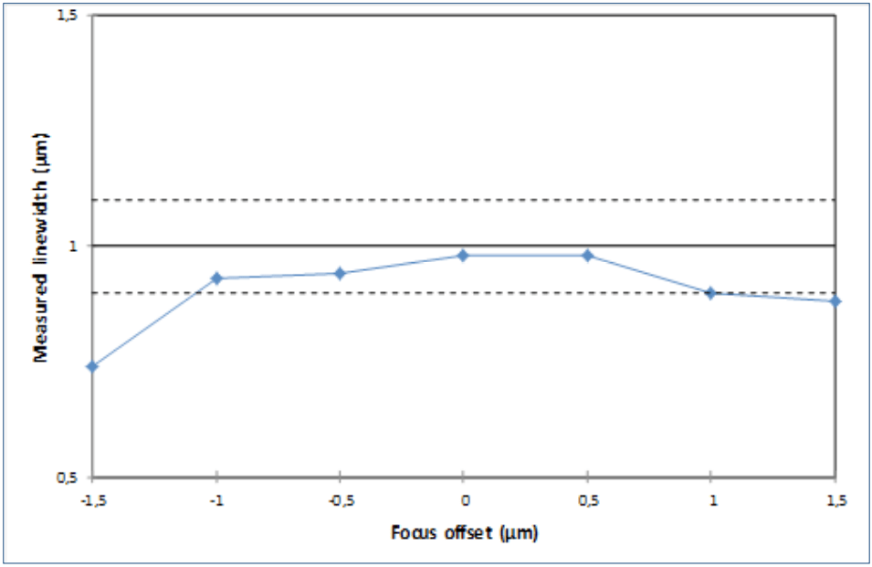
The intended structure sizes can be realized by varying the focus between -1.0 to 1.0.
Dependency of film thickness on air humidity
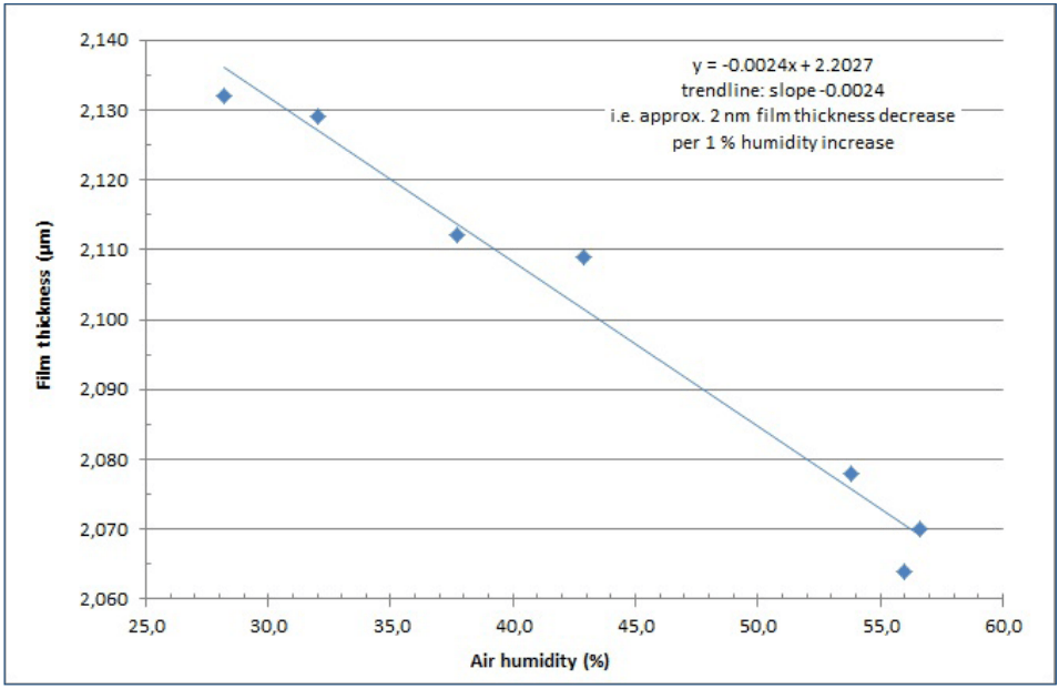
With increasing humidity, the resulting film thickness during coating of the resist decreases.
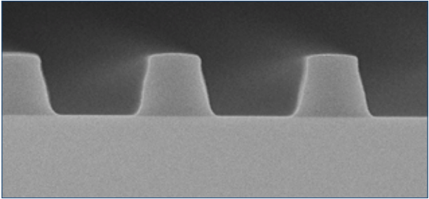
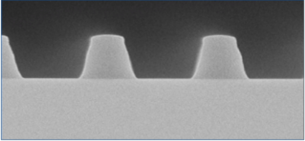
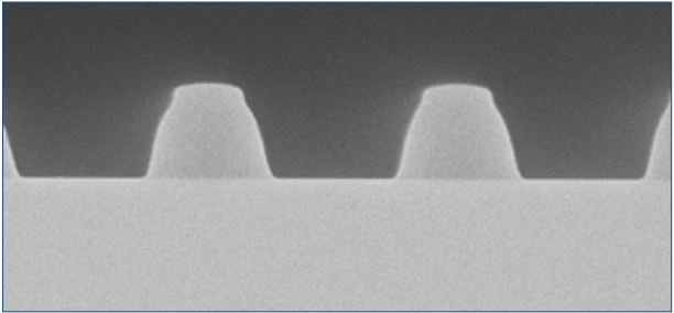
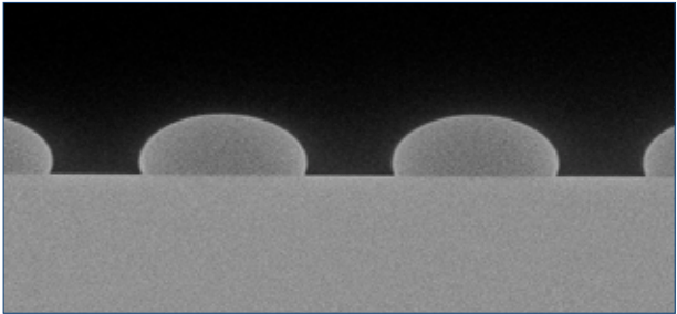
Thermal behaviour of resist structures
without hard bake
hard bake 110 °C
hard bake 120 °C
hard bake 130 °C
hard bake 140 °C
hard bake 150 °C
…
