AR-P 3500 (T) series standard positive photoresist
For semiconductor devices with wide process margin

AR-P 3500 (T) series standard positive photoresist
For semiconductor devices with wide process margin
…
AR-P 3500 series product brief 產品說明
AR-P 3500 系列產品為標準正型光阻,敏感度高,製程穩定,適合各類半導體製程。
目前產品依配方與厚度範圍有如下序號:
…
Packing & shipping 產品包裝與出貨
packing 產品包裝
✅ 250 ml/瓶
✅ 1 L/瓶
其它包裝可依需求研擬增加
shipping 產品出貨
✅ 2 – 4 週。德國運出。
❎ 1 週。國內庫存。
(目前暫無國內庫存)
本產品原廠為德國ALLRESIST GmbH. 瀏覽原廠網頁請按原廠標識。
This product is developed and produced by ALLRESIST GmbH.
Click logo to visit pricipal’s website.
…
Product features 產品特性
- broadband UV, i-line, g-line
曝光波長: 寬頻紫外線, i-line (365nm) , g-line (436nm) - high photosensitivity, high resolution
高敏感度,高解析度 - very good adhesion properties
與基板介面接著度良好 - 3500 T: robust processing, suitable for TMAH developer 0.26 n
AR-P 3510T/3540T製程穩定,適合四甲基氫氧化銨(TMAH 0.26n)顯影 - plasma etching resistant, temperature-stable up to 120 °C
耐電漿蝕刻,耐溫可達120℃ - combination of novolac and naphthoquinone diazide
主要成份為酚醛樹酯及叠氮基萘醌 - safer solvent PGMEA
使用較安全溶劑丙二醇甲醚醋酸酯
…
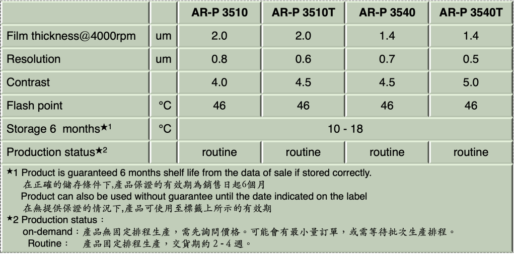
Product properties 產品物性
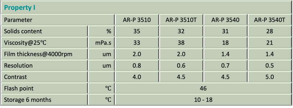
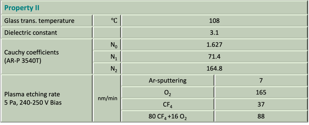
…
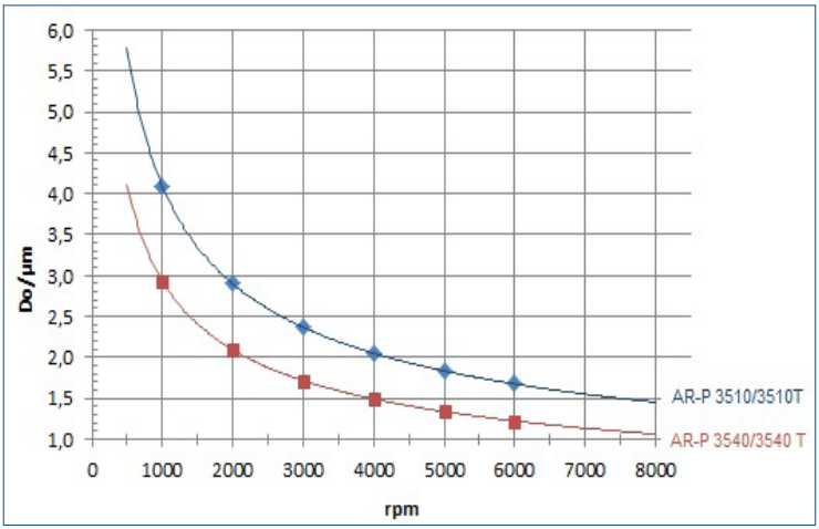
AR-P 3500 series Spin curve 塗佈曲線
…
Structure and resolution 結構與解析度
Structure resolution
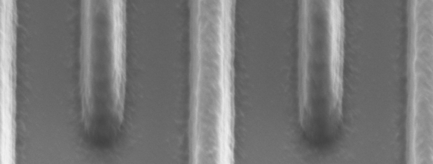
AR-P 3540 T
Film thickness 1.5 μm Resist structures 0.5 μm
Resist structure

AR-P 3540Structures without hard bake
and with tempering at 140 °C (hot plate, 1 min)
…
Process baseline 製程參數
This diagram shows exemplary process steps for AR-P 3500 series resists. All specifications are guideline values which must be adapted to own specific conditions. For further information on processing, 👉“ Detailed instructions for optimum processing of photoresists”. For recommendations on wastewater treatment and general safety instructions, 👉”General product information on Allresist photoresists”.
表列為AR-P 3500系列產品製程參數的範例。所有參數為參考值,使用者應依設備環境實際狀況加以調整。
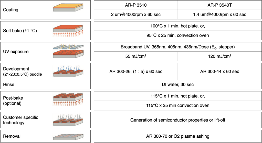
Development recipe
| Resist | Developer | ||
| AR 300-26 | AR 300-35 | AR 300-40 series | |
| AR-P 3510 / AR-P 3540 | 1 : 5 | 1 : 1 | 300-47, 1 : 1 |
| AR-P 3510T / AR-P 3540T | 1 : 2 | pure | 300-44 |
Focus width AR-P 3540 T g-line stepper
| Ridge | DOF@230mJ | Dose range |
|---|---|---|
| 1.5 um | > 2.0 um | 110 – 260 mJ/cm2 |
| 1.0 um | > 1.5 um | 130 – 260 mJ/cm2 |
| 0.7 um | > 1.25 um | 160 – 250 mJ/cm2 |
| 0.5 um | > 1.0 um | 190 – 240 mJ/cm2 |
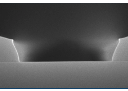
Resist structures
AR-P 3500
Film thickness 2 µm Resist structures 5 µm
…
Reference data 參考資料
Focus width
Film thickness 1.5 µm on Si-wafer, dose: 230 mJ/cm2
| Focus | 1.5 um L/S | 1.0 um L/S | 0.7 um L/S | 0.5 um L/S |
|---|---|---|---|---|
| – 1.0 | 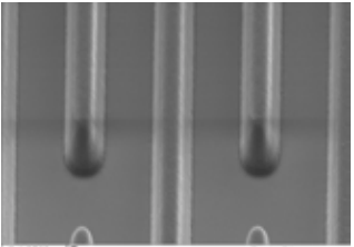 | 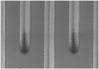 | 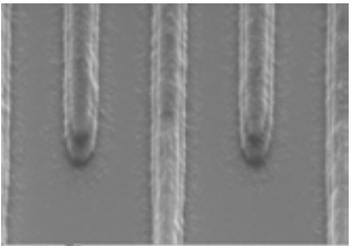 | 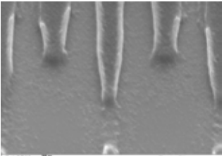 |
| – 0.75 | 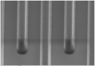 | 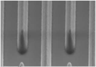 | 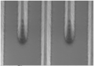 | 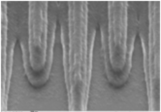 |
| – 0.5 | 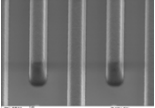 | 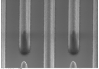 |  |  |
| – 0.25 | 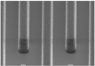 | 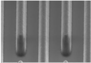 |  |  |
| 0.0 |  | 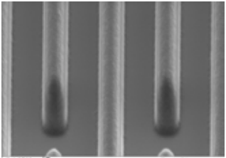 | 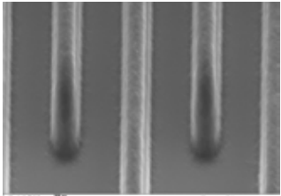 |  |
| + 0.25 | 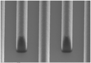 | 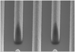 | 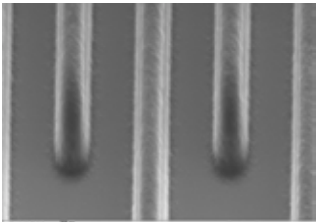 | 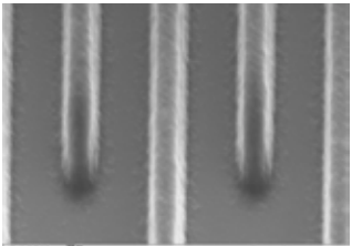 |
| + 0.5 | 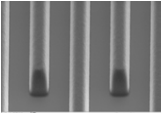 | 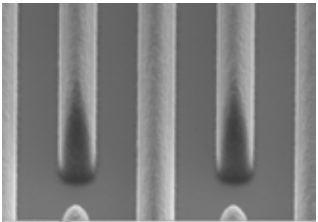 | 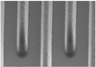 | 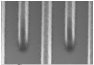 |
| + 0.75 | 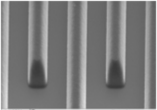 | 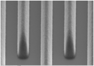 | 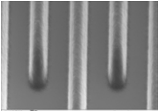 | 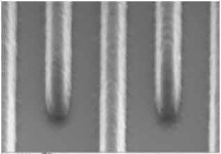 |
exposure: g-line stepper (NA: 0.56; 0.75 s)
Development: AR 300-44, 60 s, 22 °C, puddle
Linearity
Film thickness 1.5 µm on Si-wafer, focus: 0.0
| Dose | 1.5 um L/S | 1.0 um L/S | 0.7 um L/S | 0.5 um L/S |
|---|---|---|---|---|
| 160 mJ | 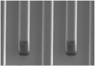 |  | 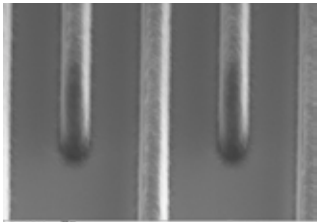 | |
| 190 mJ | 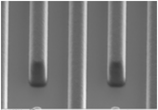 | 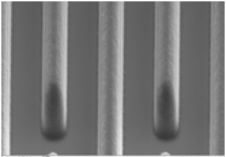 | 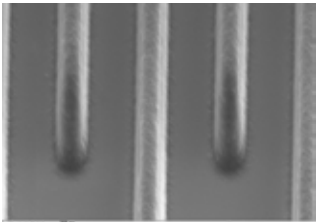 | 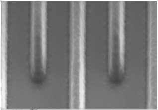 |
| 210 mJ | 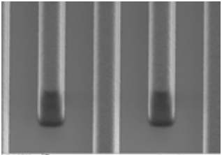 |  |  | 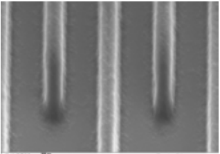 |
| 230 mJ | 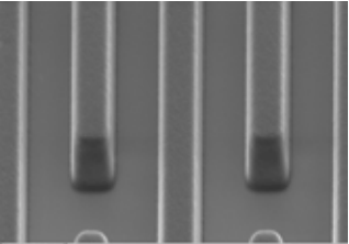 | 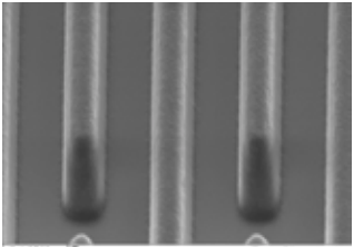 | 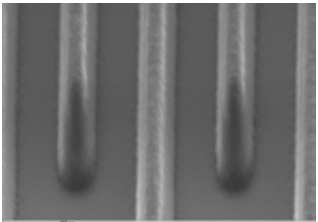 |  |
Dark field erosion
Film thickness 1.5 µm on Si-wafer, focus: 0.0
| Dose | 1.5 um L/S | 1.0 um L/S | 0.7 um L/S | 0.5 um L/S |
|---|---|---|---|---|
| 190 mJ | 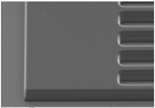 | 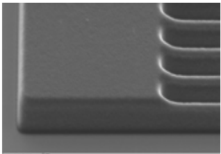 | 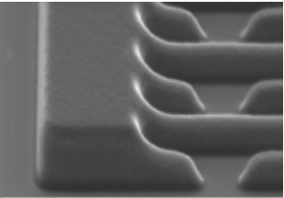 | |
| 210 mJ | 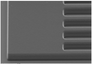 | 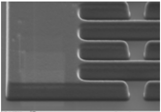 | 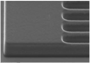 | 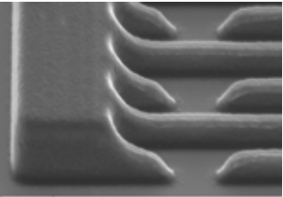 |
| 230 mJ | 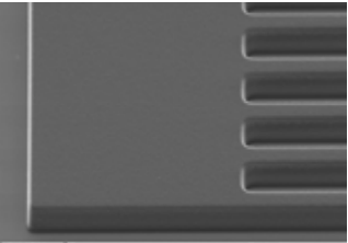 | 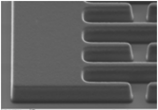 | 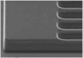 |  |
exposure: g-line stepper (NA: 0.56; 0.75 s)
Development: AR 300-44, 60 s, 22 °C, puddle
…
Contents are base on ALLRESIST product TDS.
Click logo below to link to ALLRESIST AR-P 3500 series product page .
內容取材自原廠產品技術資料,連結原廠請按下方標識。
