AR-N 4600 series (Atlas 46) for high film thickness
Negative photoresist for electroplating, micro-system and LIGA<20um
…
AR-N 4600 series product brief 產品說明
AR-N 4600系列,實驗代號Atlas 46,為高膜厚產品,適合於電鍍,微系統,微機電等各類應用。
產品編號: AR-N 4610 (S) – stable layer. 可做為結構的一部份。
AR-N 4650 (R) – removable layer. 適合於各類金屬電鍍製程。
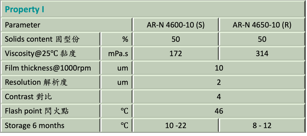
產品基本資料如下:
| unit | AR-N 4600-10 (S) (permanent film) | AR-N 4650-10 (R) (removable film) | |
|---|---|---|---|
| Viscosity@25℃ 黏度 | mPa.s | 172 | 314 |
| Film thickness@1000rpm | um | 10 | 10 |
| Resolution 解析度 | um | 2 | |
| Contrast 對比 | 4 | ||
| Flash point 閃火點 | ℃ | 46 | |
| Storage 6 months | ℃ | 10 – 22 | 8 – 12 |
| Production status1 | routine | on-demand | |
| 1. Production status: on-demand:產品無固定排程生產,需先詢問價格。可能會有最小量訂單,或需等待批次生產排程。 Routine: 產品固定排程生產,交貨期約2-4週。 | |||
…
Packing & shipping 產品包裝與出貨
packing 產品包裝
✅ 250 ml/瓶
✅ 1 L/瓶
其它包裝可依需求研擬增加
shipping 產品出貨
✅ 2 – 4 週。德國運出。
❎ 1 週。 國內庫存。(本產品暫無國內庫存)
AR-N 4650-10無固定排程生產,需先詢問。
…
Product features 產品特性
- i-line, broadband UV
曝光波長: 寬頻紫外線, i-line (365nm) - very good adhesion properties
黏著度良好 - very high sensitivity
光阻具高敏感度 - 4600-10 for stable layers of 5 μm – 15 μm
AR-N 4600-10應用於 厚度 5 um – 15 um的永久材 - 4650-10 for removable layers of 5 μm – 15 μm
AR-N 4650-10應用於厚度 5 um -15 um的可去除光阻 - further film thicknesses up to about 200 μm available on request
厚度可依需求調整,最高可達200 um。 如有需要請連絡 - poly[(o-cresyl glycidyl ether)-co-formaldehyde] and acid generator
成份含PCGF-聚[(鄰甲苯基縮水甘油醚)-共甲醛]與光酸 - safer solvent PGMEA
使用較安全溶劑丙二醇甲醚醋酸酯
…
Product properties 產品物性
…
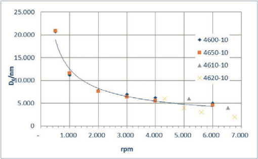
AR-N 4600 series Spin curve 塗佈曲線
…
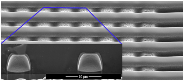
Structure and resolution 結構與解析度
Resist structure
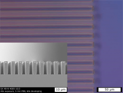
Atlas S (© Martin-Luther-Universität Halle-Wittenberg)
Resist structure
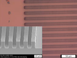
Atlas R (© Martin-Luther-Universität Halle-Wittenberg)
…
Process baseline 製程參數
This diagram shows exemplary process steps for AR-N 4600 series photoresists. All specifications are guideline values which must be adapted to own specific conditions. For further information on processing, 👉“ Detailed instructions for optimum processing of photoresists”. For recommendations on wastewater treatment and general safety instructions, 👉”General product information on Allresist photoresists”.
表列為AR-N 4600 系列產品製程參數的範例。所有參數為參考值,使用者應依設備環境實際狀況加以調整。
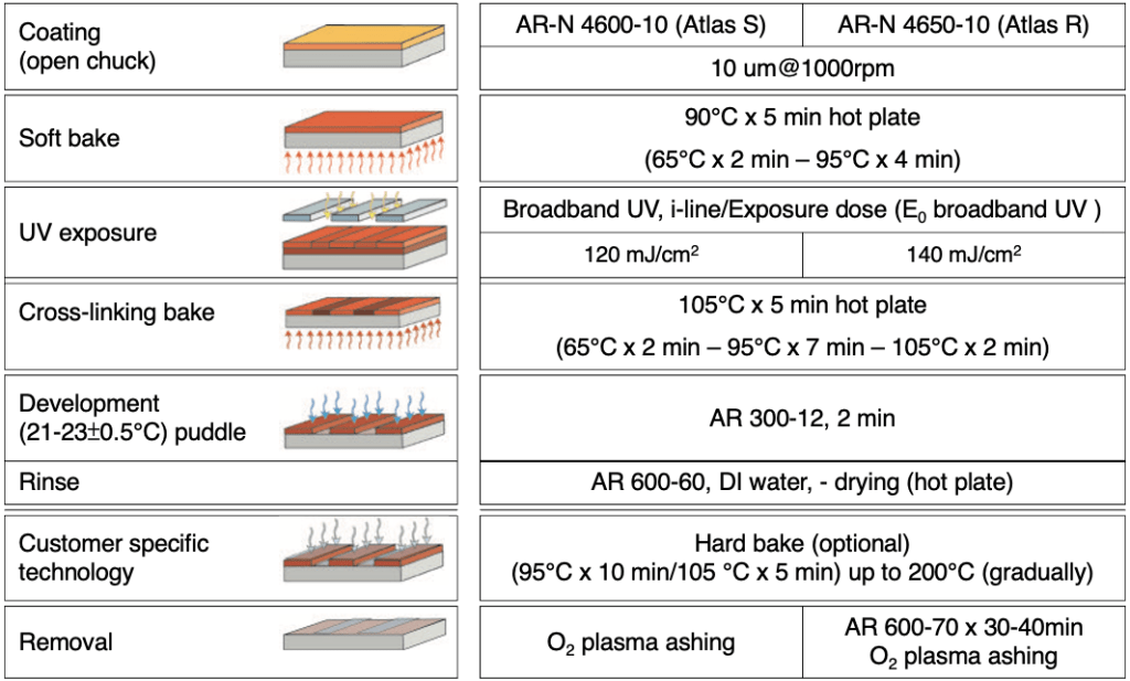
Development recipe
| Developer | Resist | |
| AR-N 4600-10 | AR-N 4650-10 | |
| AR 600-70 | fast | fast |
| AR 300-12 | middle | middle |
| AR 600-07 | slow | sloe |
…
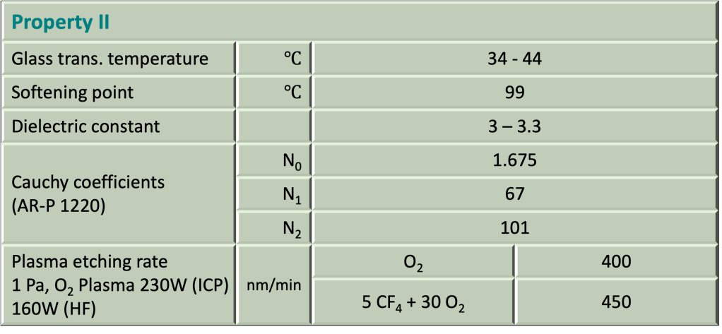
Reference data for process tuning
UV/VIS NIR
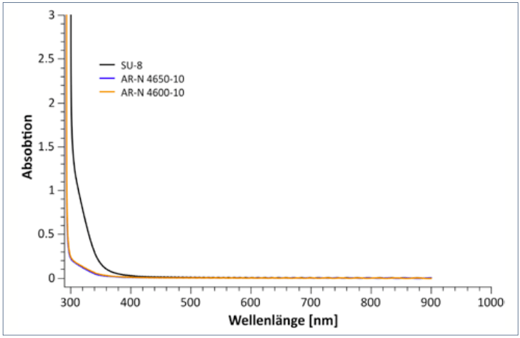
UV/VIS spectra of 10 μm layers Atlas S and Atlas R in comparison to SU-8
UV/VIS NIR

UV/VIS spectra of Atlas 46. Yellowing caused by varying the dura- tion of broadband UV exposure after curing.
…
Imprinting
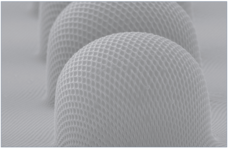
Combined nano- and microstructures, produced by imprinting of AR-N 4600 (© Uni Wuppertal)
Imprinting
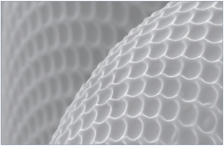
Close-up view of AR-N 4600 (© Uni Wuppertal)
…
DSC
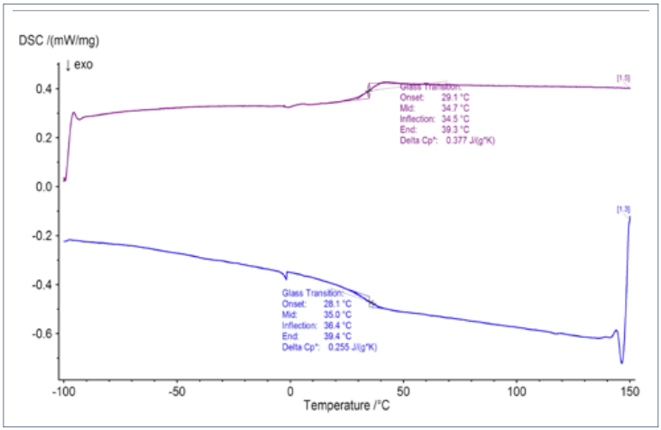
DSC of Atlas S (AR-N 4600-10)
DSC
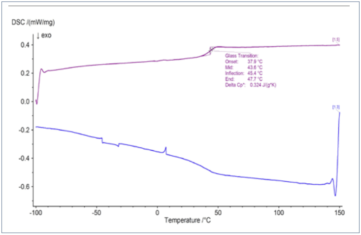
DSC of Atlas R (AR-N 4650-10)
…
Bridge application
Bridge structure of two-layer system with
AR-N 4600-10 (bottom) and SX AR-N 4620-10/1 (top)
Bridge application
Process description of “bridge construction” with AR-N 4600-10 (bottom, BB-UV) and SX AR-N 4620-10/1 (top, g-line)
…
Addtional information for process
Layer thickness values of Atlas R and Atlas S are pre- adjusted to 10 μm at a spin speed of 1000 rpm. It is re- commended to perform the subsequent tempering step on the hotplate at 95 °C for 5 min. Temperature ramps or stepwise drying, e.g. 65 °C for 2 minutes, followed by 95 °C for 4 minutes, can improve the resolution.
Both resists can be structured by i-line or broadband UV exposure. Prior to irradiation, substrates should be cooled to room temperature. It is recommended to per- form the following tempering step for cross-linking on the hotplate at 105 °C for 2 min.
Ramps or stepwise cross-linking procedures like e.g. 65 °C for 2 minutes, followed by 95 °C for 7 minutes and 105 °C for 2 minutes, can improve the resolution. In general, the stability of resists increases with higher tem- peratures and longer bake times, but this requires on the other side longer development times. The use of tem- perature ramps is also recommended for cooling since cooling too fast may result in stress cracking.
Atlas R及Atlas S的厚度是事先調整為轉速1000 rpm時為10um。 接著建議以熱板加熱95℃x5min。 階梯式升溫可改善解析度,例如: 65℃ x 2 min, 再以95℃ x 4 min。
Atlas R及Atlas S曝光波長為寬頻紫外線(broadband UV)或365nm (i-line)。 曝光前,晶片應先冷卻至室溫。 曝後烤建議溫度時間為:105℃ x 2min (熱板)。 階梯式曝後烤亦可改善解析度,例如:65℃ x 2 min, 95℃ x 7 min, 105℃ x 2 min。 ㄧ般而言,較高溫度與較長烘烤時間可增加光阻的穩定度,但同時也需要較長的顯影的時間。
晶片冷卻時也建議採階梯式降溫,可避免因降溫速度過快,光阻因應力而產生裂痕。
Development 顯影
AR 300-12 is recommended as standard developer, but also AR 600-07 (fast development) or AR 600-70 (gentle development) is suitable. If AR-N 4600-10 (S) is used for development, no dark erosion is observed even after comparably long development times. If the development with AR 300-12 is performed for too long, increased dark erosion of AR-N 4650-10 may result, and a too long development with AR 600-70 can even cause complete removal.
Stopper AR 600-60 is recommended for a particularly residue-free rinsing after development, followed by rin- sing with DI water. It is also possible to rinse resist layers immediately after development directly with DI water and to dry them on the hotplate.
The sensitivity for a layer thickness of 10 μm is about 110 – 160 mJ/cm2 in the broadband UV range (process description on page 3).
顯影劑一般建議使用AR 300-12。但AR 600-70(顯影速度快)及AR 600-07(顯影速度慢)ㄧ樣適用。AR-N 4600-10(S)即使在長的顯影時間也觀察不到顯影劑對光阻蝕刻的問題.
AR-N 4650-10(R)如果在AR 300-12顯影時間過長,就容易發生顯影劑對光阻蝕刻現象, 在AR 600-70顯影時間過長,甚至會使光阻去除。
AR 600-60建議使用於顯影後,接著再以DI water潤洗。 也可以顯影後直接以DI water潤洗,再以熱板乾燥。
曝光敏感度大約是:10um厚度於寬頻紫外線110 – 160 mJ/cm2
Removal 光阻去除
Coated structures of AR-N 4650-10 (R) can be remo- ved with thinner AR 300-12 or AR 600-70. Depending on the degree of cross-linking (dose, temperature and bake time), required removal times may be considerably longer than 30 minutes.
AR-N 4650-10(R)的結構可被AR 300-12或AR 600-70去除。 依阻劑架橋程度(曝光劑量,烘烤溫度與時間),一般去除時間會超過30分。
…
Dyed and fluorescent films with Atlas 46
Different coloured, optionally also fluorescent dyes can be embedded into the negative-working Atlas 46 S. These dyes are process-stable, and structuring is performed in the same manner as in standard processes with uncolored Atlas 46 S films.
Atlas 46(S)負型光阻可加入不同顏色染料或螢光染料. 製程穩定,與未加染料時的參數一樣. 圖示為5um膜厚加入不同顏色的公司標示.
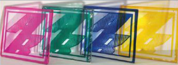
Vary-colored company logo with Atlas 46 S, film thickness 5 μm
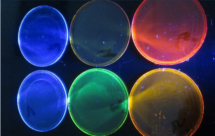
Differently fluorescing Atlas 46 films (irradiation with black light)
The use of different fluorescent dyes allows a defined adjustable emission in variable wavelength ranges. Fluorescent resist films are e.g. applied in microscopy. By embed- ding dyes into Atlas 46 S, resist films can be created that optionally show violet, blue, green, yellow, orange or red fluorescence. The intense fluorescence is retained even after a tempering at 150 °C, and the intense UV exposure required for cross-linking of Atlas films exhibits no adverse effect on the emission properties of these layers.
螢光染料可依需求調整不同波長的螢光.俱螢光反應的光阻膜,例如在顯微鏡的應用. 在Atlas 46(S)中加入螢光染料,依需求可顯示紫色,藍色,綠色,黃色,橘色或紅色.螢光的強度及特性不會受到製程中加熱150℃,及紫外光曝光,高分子架橋等因素影響
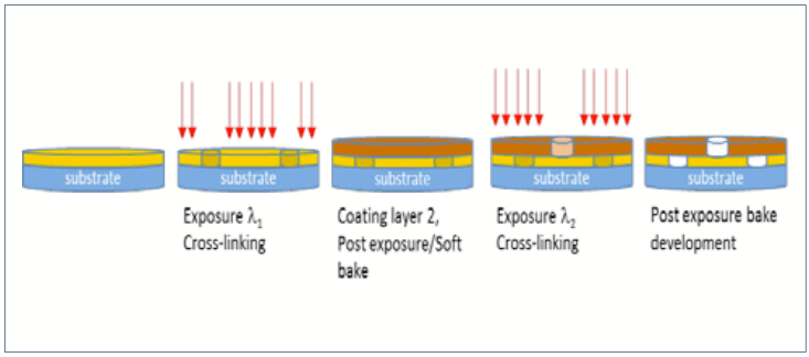
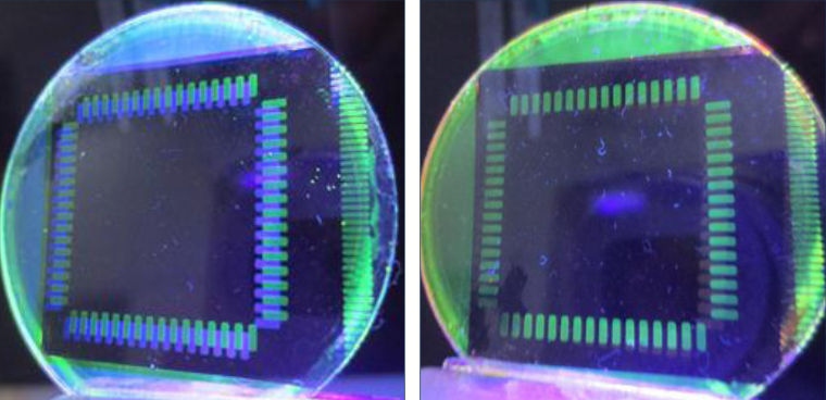
Also two-color fluorescent resist architectures could be realized. For this purpose, glass panes were pre-treated with AR 300-80new to optimize the adhesive properties and subsequently coated with different fluorescent Atlas 46 S variants. Exposure was carried out using different masks. After the following PEB, development was carried out with AR 300-12 and films were dried. The developed structures were then coated with a second, differently colored resist variant with the greatest possible color contrast, e.g. blue – yellow or red – yellow.
No mixing occurred since the already produced structures turned out to be highly stable. The second exposure and PEB step analogous to the first step allowed a selective structuring of the upper layer. After development with AR 300-12, the differently fluorescing areas on the substrate become visible in black light:
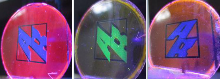
AR logo realised with two-colored emission in black light
雙色螢光製程:玻璃基板先以AR 300-80new以增加黏度, 再塗佈參雜不同螢光染料的Atlas 46(S). 接著以不同光罩進行曝光. 曝後烤後以AR 300-12進行顯影並乾燥. 緊接著進行第二層不同顏色的製程. 顏色選擇儘量以最大對比的組合,例如:藍-黃,或,紅-黃.
兩段製程各自形成穩定的結構,不會有混合的情況. 第二段製程的曝光及曝後烤可再上層形成選擇性結構,以AR 300-12顯影後就可形成不同顏色的發光區域.
Different fluorescent line patterns, left: parallel arrangement, right: overlapping lines
Also differently fluorescent lines adjacent to each other (or optionally overlapping) can be created in the same way:
相鄰或重疊的螢光線條也可以此製程製作。
…
