AR-N 4400 series Negative Thick Layer photoresist (CAR 44)
For the application of electroplating, micro-system and LIGA
…
AR-N 4400 series product brief 產品說明
AR-N 4400系列(CAR 44)為高膜厚光阻,適合電鍍,微系統,微機電等各類應用。
產品基本資料如下:
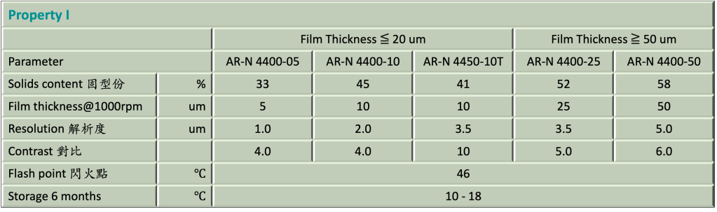
| Unit | AR-N 4400-05 | AR-N 4400-10 | AR-N 4450-10T | AR-N 4400-25 | AR-N 4400-52 | |
|---|---|---|---|---|---|---|
| Film thickness 1000 – 250 rpm | um | 5 – 10 | 10 – 20 | 10 – 20 | 25 – 50 | 50 – 100 |
| Resolution | um | 1.0 | 2.0 | 3.5 | 3.5 | 5.0 |
| Contrast | 4.0 | 4.0 | 10 | 5 | 6 | |
| Flash point | ℃ | 46 | ||||
| Storage 6 months1 | ℃ | 10 – 18 | ||||
| Production status2 | routine | routine | on-demand | routine | routine | |
| GHS label | 📎 GHS標識 | 📎 GHS標識 | 📎 GHS標識 | 📎 GHS標識 | 📎 GHS標識 | |
| 1. Product is guaranteed 6 months shelf life from the data of sale if stored correctly. 在正確的儲存條件下,產品保證的有效期為銷售日起6個月。 Product can also be used without guarantee until the date indicated on the label. 在無提供保證的情況下,產品可使用至標籤上所示的有效期。 2. Production status: on-demand:產品無固定排程生產,需先詢問價格。可能會有最小量訂單,或需等待批次生產排程。 routine: 產品固定排程生產,交貨期約2-4週。 | ||||||
…
Packing & shipping 產品包裝與出貨
packing 產品包裝
✅ 250 ml/瓶
✅ 1 L/瓶
其它包裝可依需求研擬增加
shipping 產品出貨
✅ 2 – 4 週。德國運出。
❎ 1 週。 國內庫存。(本產品暫無國內庫存)
AR-N 4450-10T無固定排程生產,需先詢問。
…
Product features 產品特性
- broadband UV, i-line, g-line, e-beam, X-ray, synchrotron
適合各類曝光;寬頻紫外線, i-line, g-line, 電子束,x光,同步輻射 - chemically enhanced, very good adhesion, electro plating-stable
化學放大型光阻. 與基板介面接著性良好. 於電鍍製程穩定 - very high sensitivity, easy removal
光阻具高敏感度,且去除容易 - profiles with high edge steepness for excellent resolution, covering of topologies
光阻圖案側視具垂直邊緣,解析度高 - 4400-05 for film thicknesses up to 10 μm (250 rpm)
4400-05膜厚在250轉可達10um - 4400-10 for film thicknesses up to 20 μm (250 rpm)
4400-10膜厚在250轉可達20um - 4450-10T for film thicknesses up to 20 μm and lift-off, developing by TMAH 0.26n
4450-10T膜厚在250轉可達20um,適lift-off及TMAH (0.26n)顯影 - 4400-25 for very thick film up to 50um (250 rpm)
4400-25膜厚在250轉可達50um - 4400-50 for highest film thickness up to 100 um
4400-50膜厚可達100um - novolac, crosslinking agent, amine-based acid generator
成份含酚醛樹脂,架橋劑,胺基光酸 - safer solvent PGMEA
使用較安全溶劑丙二醇甲醚醋酸酯
…
Product properties 產品物性
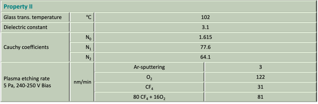
…
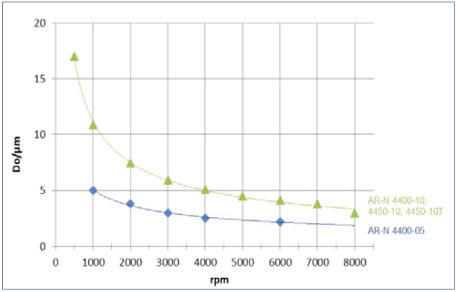
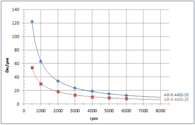
AR-N 4400 series Spin curve 塗佈曲線
Spin curve od AR-N 4400-05/10/10T
Spin curve od AR-N 4400-25/50
…
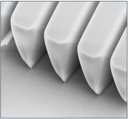
Structure and resolution 結構與解析度
Structure resolution
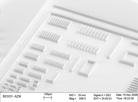
AR-N 4400-10 3um resolution at a film thickness of 15um
Resist structure
Turbine wheel produced with AR-N 4400-10
Process parameters
| Substrate | Si 4″ wafer |
| Soft bake | 95℃ x 10 min, hot plate |
| Exposure | Mask aligner MJB 3, contact exposure |
| Development | AR 300-47x 3min, 22℃ |
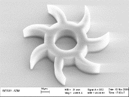
Structure resolution
AR-N 4400-25 5um trench at a film thickness of 40um
Resist structure
Siemens star produced with AR-N 4400-25 (30um thick)
…
Process baseline 製程參數
This diagram shows exemplary process steps for AR-N 4400 series photoresists. All specifications are guideline values which must be adapted to own specific conditions. For further information on processing, 👉“ Detailed instructions for optimum processing of photoresists”. For recommendations on wastewater treatment and general safety instructions, 👉”General product information on Allresist photoresists”.
表列為AR-N 4400 系列產品製程參數的範例。所有參數為參考值,使用者應依設備環境實際狀況加以調整。
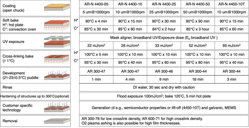
Development recipe
| Developer | Resist | ||||
| AR-N 4400-05 3 – 10 um | AR-N 4400-10 5 – 20 um | AR-N 4400-25 13 – 25 um | AR-N 4400-50 25 – 100 um | AR-N 4450-10T 5 – 20 um | |
| AR 300-44 | – – | – – | – – | 8 : 1 – pure | pure |
| AR 300-46 | – – | – – | 5 : 1 – pure | pure | – – |
| AR 300-47 | 6 : 1 – pure | 3 : 2 – pure | pure | – – | – – |
| AR 300-475 | pure | – – | – – | – – | – – |
…
Reference data for process tuning
Sensitivity of AR-N 4400-05
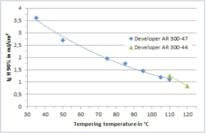
The sensitivity increases constantly with increasing bake temperatures (broadband UV Mask aligner, thickness 5.0 μm)
Time for complete development of AR-N 4400-05
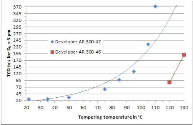
With increasing temperature, the TCD increases considerably. > 130 °C, no development is possible even if strong developers (AR 300-44) are used.
…
Gradation of AR-N 4400-05
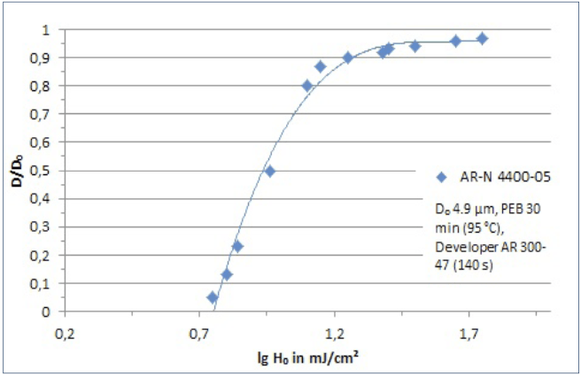
The gradation (contrast) is 3.5, the sensitivity was determined to 21.5 mJ/cm2 for a structure buildup of 90 % (H090).
Thermal stability and shrinkage up to 300℃
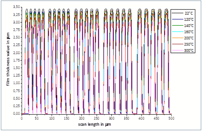
Developed lines with a width of 10 – 20 μm were hardened by flood exposure and subsequent bake step. These lines were tempered stepwise until 300 °C. Up to a temperature of 200 °C, structures remain more or less unchanged.
…
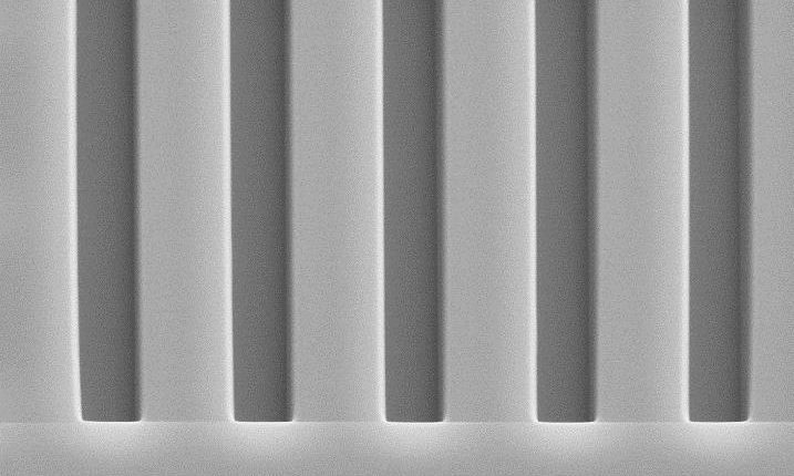
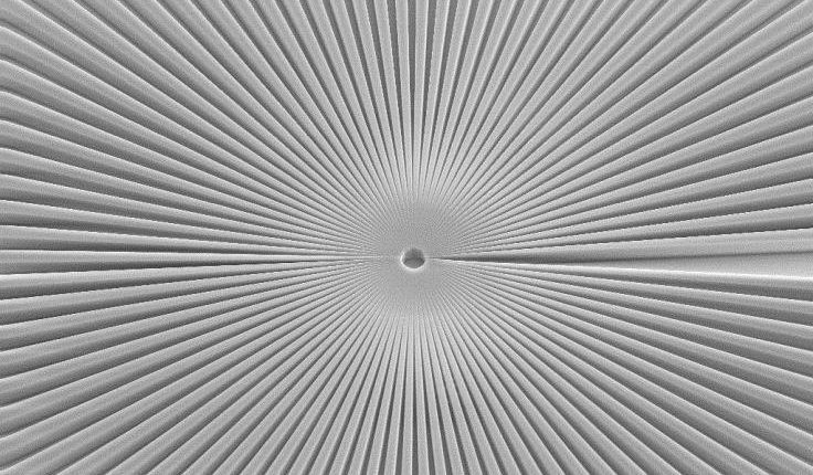
Resolution of AR-N 4400-05
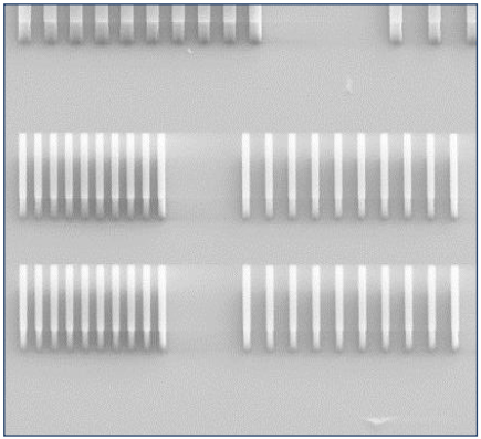
At a film thickness of 5 μm, 1.0 μm bars were produced
Picture of Einstein

Test structure produced on the occasion of the “Einsteinjahr” in 2006
Lift-off structure
Undercuts produced with low exposure dose (AR-N 4450-10T)
…
Process recipe for thick layer
Coating
In order to avoid the formation of bubbles, the resist should be left undisturbed for at least one day prior to processing. For resist with higher viscosity from AR-N 4400-25 onwards, degassing with ultra- sound or vacuum is advisable.
The resist should be applied slowly, from a low height and always using the same amount of resist (e.g. 100 ml for 4-inch-wafers) onto the standing wafer. Subsequently, a formation for 10 s a low rotational speed (250 – 400 rpm) is recommended, followed by slow in- crease of the spin speed up to the desired final speed. To achieve a high resist film quality, rotational speeds above 2000 rpm should be avoided for the highly viscous AR-N 4400-50.
👉 Shorter coating times at final spin speed will increase the film thickness.
Multiple coating steps (up to 4 x) are possible for film thicknesses between 50 and 150 μm. A particularly high edge steepness of structures results in this case from an improved drying procedure. After each coa- ting step, the resist is dried at 85 °C (hot plate) or 90 °C (convection oven) according to the specifications as given in the process conditions.
塗佈:
為避免氣泡形成,塗佈前光阻應先靜置至少一天。 高黏度光阻,例如AR-N 4400-25以上,建議以超音波或真空脫氣。
光阻滴膠應儘量接近基板,滴膠速度不要太快且保持定量。 例如:定量100ml於4寸晶圓。滴膠先以低轉速(約250 – 400rpm)讓膠膜成型,再依厚度需要,逐步增加轉速。高黏度光阻,例如AR-N 4400-50,為維持厚膜品值,應避免轉速超過2,000 rpm。減少主轉速塗佈時間,可提高膜厚。
介於50 – 150 um的高膜厚可以多次塗佈達成。 改善軟烤程序可讓高膜厚光阻圖案邊緣垂直度增加。 如前製程基本參數所述:在各個塗佈程續後以 85℃(熱板)或90℃對流烤箱對光阻軟烤。
Tempering 軟烤
The required tempering times are highly dependent on the respective film thickness:
軟烤的時間與光阻厚度有直接關係:
| Thickness | drying time (hot plate) | drying time (convection oven) |
|---|---|---|
| 10 um | 10 min | 1 hour |
| 25 um | 45 min | 4 hour |
| 50 um | 90 min | 7 hour |
The use of temperature ramps is highly recommended, since too fast cooling may lead to tension cracks.
👉 Long intensive drying procedures result in decreased sensitivities and prolonged development times.
建議階梯式升降溫以避免光阻冷卻過快導致應力破裂。長時間,高強度乾燥會降低敏感度及拉長顯影時間。
Cross-linking:
The crosslinking temperature can be varied in the range from 85 °C to 105 °C. The bake can be performed a few days after exposure without loss of sensitivity.
👉 Higher temperatures lead to a slower development.
架橋:
光阻架橋溫度介於85℃至105℃之間。 此程序於執行曝光後幾天內,不至於降低其敏感度.。高溫架橋(曝後烤)會導致顯影變慢。
Development:
longer development times with weaker developer provide a higher imaging quality. For AR-N 4450-10T, the undercut (lift-off) of resist structures can be achieved by extending the development time at the minimum required exposure dose.
顯影:
以較弱顯影劑拉長顯影時間可得到較佳圖案品值。
AR-N 4450-10T以低劑量曝光並拉長顯影時間可獲得下切型結構。
Removal:
Crosslinked structures can easily be removed by wet- or plasma chemical procedures using removers AR 600-71 and AR 300-76. Complicated electroplating structures as well as substrates treated with high temperatures require removers AR 600-71 or AR 300-70.
光阻去除:
光阻經架橋後形成的結構可以去除劑AR 600-71, AR 300-76或電漿去除。
基板上的光阻結構用於金屬電鍍則需AR 600-71或AR 300-70去除劑。
…
Comparison – CSAR 44 vs rival
| CSAR 44 | Resist properties – Suitability 光阻物性-適用性 | Sx-xx |
| ✅ | thick films 厚膜光阻特性 | ✅✅ |
| ✅ | high resolution 解析度 | ✅ |
| ✅ | excellent aspect ratio 深寬比 | ✅ |
| ✅ | high sensitivity at i-line, deep UV, e-beam, X-ray 各類光源曝光敏感度 | ✅✅ |
| ✅ | good sensitivity at g-line g線波長曝光敏感度 | ❎ |
| ✅ | low-stress tempering – easy handling 低熱應力-製程控制性 | ❎ |
| ✅ | aqueous-alkaline development 鹼性水溶液顯影 | ❎ |
| ✅ | easy removal 光阻去除性 | ❎ |
…
