Product is guaranteed 6 months shelf life from the date of sale if stored correctly.
在正確儲存條件下,產品保證的有效期限為銷售日起6個月。
Product can also be used without guaranteed until the date indicated on the label.
在無提供保證的情況下,產品可使用至標籤上所示的有效期。
*2
Production status:
routine:產品固定排程生產,交貨期約2-4週。
on-demand:產品無固定排程生產,需先詢價。可能有最小訂購量(MOQ)或需待批次生產排程。
*3
Product code 產品編碼說明:
…
Product Features 產品特性
e-beam, deep UV (248 nm) 阻劑可於電子束, 深紫外線下曝光
very good adhesion to glass, silicon and metals 阻劑與玻璃, 矽及金屬的粘著度良好
50K 20 % more sensitive than 950K 分子量50k的產品,其敏感度比950k的優約20%
for planarization and multi-layer processes 適合於平坦化及多層電路製程
highest resolution, high contrast 產品具高解析度及高對比
poly(methyl methacrylate) with different molecular weights 高分子為不同分子量的PMMA (聚甲基丙烯酸甲酯)
Type of solvent for different molecular weight: 各產品編號使用的溶劑如下: AR-P 631-671 solvent chlorobenzene,(氯苯) flash point 28 °C AR-P 632-672 safer solvent anisole, (苯甲醚)flash point 45.5 °C AR-P 639-679 safer solvent ethyl lactate,(乳酸乙酯) flash point 36 °C
…
Product Properties 產品物性
Property I
unit
Product code AR-P
631-639
641-649
661-669
671-679
Molecular weight 分子量
50k
200k
600k
950k
Film thickness@4000rpm
um
20 – 310
20-780
20-1,040
30-1,870
Solid content 固型份
%
1 – 12
1 – 12
1 – 11
1 – 11
Resolution (best) 最佳解析度
nm
6
Contrast 對比度
7
Storage 6 months*1
10 – 18 ℃
Property II
unit
Glass transition temp. (Tg)
℃
105
Dielectric constant 介電常數
2.6
Cauchy coefficients
N0
N1
N2
1.478
47.3
0
Plasma etching rate (5Pa, 240 – 250 V Bias)
AR-sputtering
nm/min
21
O2
nm/min
344
CF4
nm/min
59
80 CF4 + 16 O2
nm/min
164
…
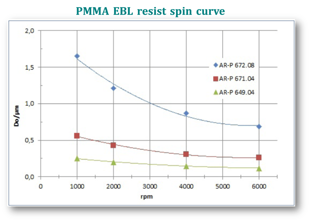
Spin Curve 塗佈曲線
…
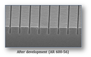
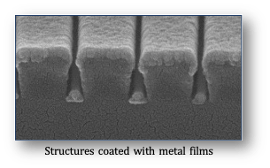
Resist Structure and Resolution結構解析度
Structure resolution
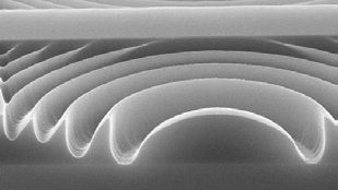
AR-P 679.02 Structural resolution: 6.2 nm gap, 65 nm high
Resist structure
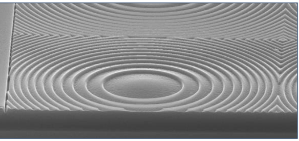
AR-P 671.09 diffractive optics, thickness of 4.4 μm
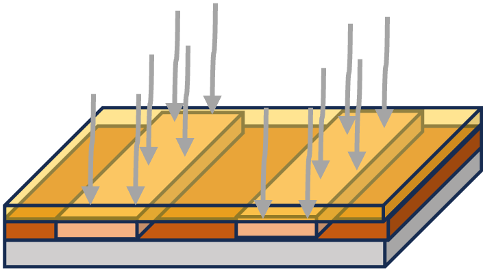
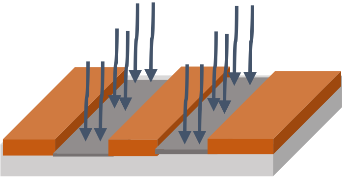
This diagram shows exemplary process steps for resists of AR-P 630 – 670 series. All specifications are guideline values which must be adapted to own specific conditions. For further information on processing, 👉“Detailed instructions for optimum processing of e-beam resists”. For recommendations on wastewater treatment and general safety instructions, 👉”General product information on Allresist e-beam resists”.
圖示AR-P 630-670 series PMMA阻劑產品製程參數的範例. 所有參數為參考值,使用者應依設備環境實際狀況加以調整
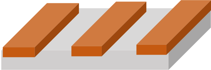
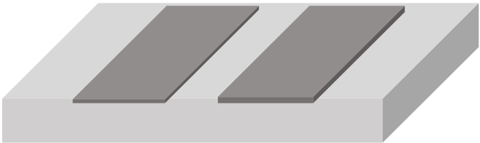
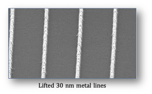
Processing instructions for coating Large undercut structures (lift-off) are obtained if PMMA resists with different molecular weight are chosen for a two-component system. As upper layer, an ethyl lactate PMMA is recommended since ethyl lactate does not, in contrast to other solvents, attack the second layer. For the lower layer, a chlorobenzene, anisole or ethyl lactate PMMA is suitable. Both tempering steps are performed at 150 °C.
Recommendation: large undercut (low resolution): bottom layer 50K, upper layer 200K, 600K or 950K. High resolution (smaller undercut): bottom layer 600K, upper layer 950K.
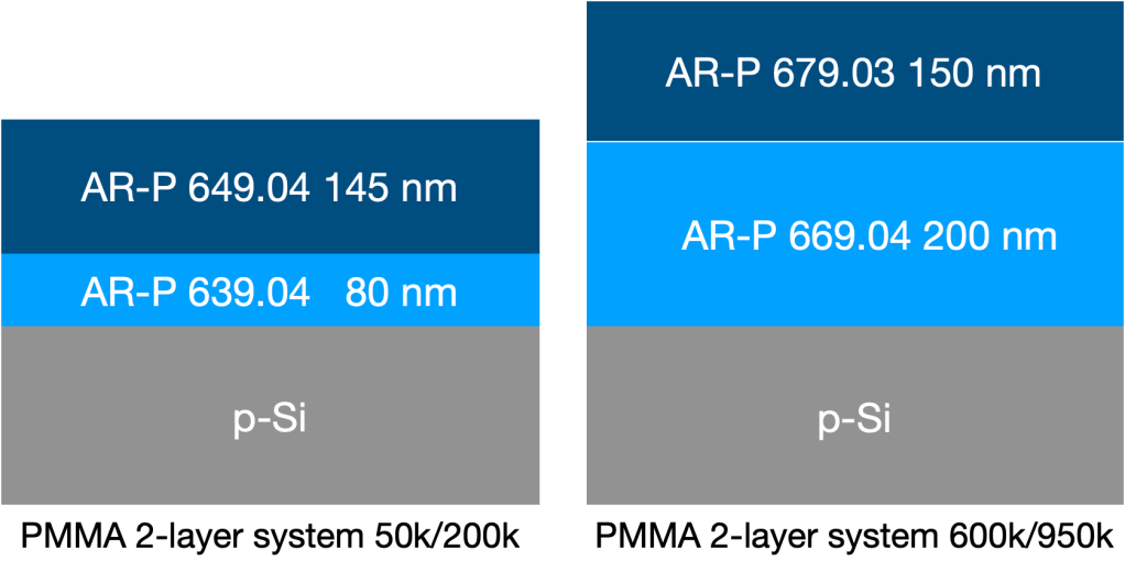
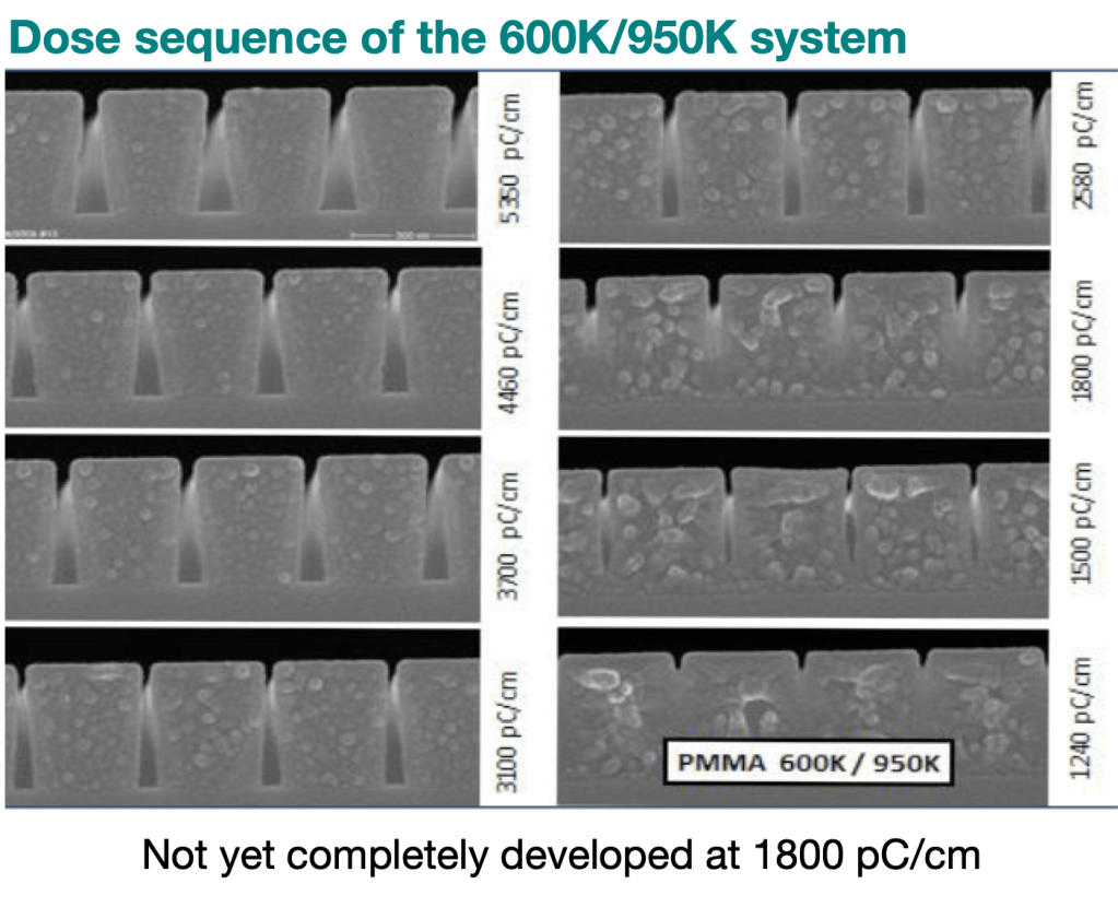
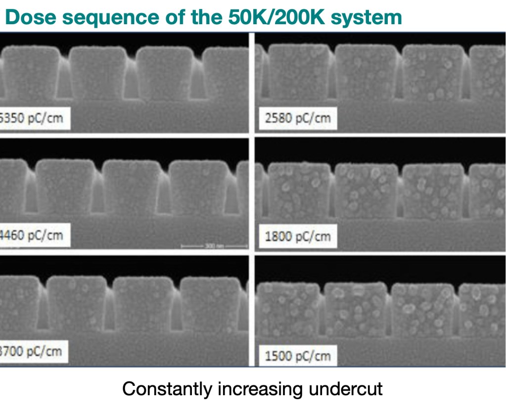
Investigations of 2-layer PMMA lift-off structures 雙層組合範例
or these tests, the 2-layer systems were coated as shown to the below and tempered at 180℃, 60 s, followed by irradiation with different doses (30 kV) and development (AR 600-60, IPA). 雙層組合結構的組合測試,(如圖),塗佈後以180℃軟烤,再以30kV加速電壓在不圖劑量下曝光後顯影(AR 600-60, IPA)
The system 50K/200K is more sensitive, the double layer is completely developed at 1500 pC/cm2. The variant 600K/950K in contrast requires the higher dose of 2200 pC/cm2. With increasing dose, also a larger undercut is generated if the 50K/200K system is used, which is thus predestined for complicated lift-off procedures. Variant 600K/950K may be utilised for higher total film thicknesses (> 500 nm) and is a reliable lift-off system for simple applications. For these investigations, always AR 600-60 (IPA) was used as developer which explains both the comparably high doses and the good process stability. 分子量 50k/200k的組合,其敏感度較高,雙層完全顯開約需1500 pC/cm的曝光能量. 分子量 600k/950k則需2200pC/cm的較高劑量. 複雜的懸浮剝離製程,一般先以50k/200k的組合, 增加曝光劑量可獲得較大的下切結構. 600k/950k的組合,則應用於膜厚需求較高的製程(>500nm). 這些研究皆以AR 600-60(IPA)為顯影劑,因此需要較高的曝光劑量,但製程相當穩定.
Sensitivity of PMMA resist
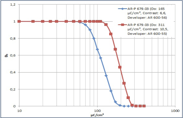
The diagram below shows a comparison of the sensitivity of AR-P 679.03 in two different developers. Under otherwise identical conditions (30 kV, 165 nm film thickness), the sensitivity is almost twice as high if the standard developer AR600-55 is used as compared to AR 600-60 (IPA). A development with IPA however results in a considerably higher contrast (10.5 : 6.6). This developer is thus predestined for higher resolutions. Experience furthermore shows that the process window is significantly larger as compared to faster developers. Dose deviations of e.g. 10 % are tolerated without any quality loss. 下圖以AR-P 679.03為例顯示在2種不同顯影劑下的敏感度的比較. 在相同參數條件下(30kV, 165nm film thickness), 使用顯影劑AR 600-55比AR 600-50 (IPA),敏感度高出2倍. 然而使用IPA顯影有高對比的特性(10.5:6.6). 因此IPA用於較高解析度的製程. 實驗也顯示其製程穩定度高於快速顯影的製程. 10%的曝光劑量偏差不會影響製程品質
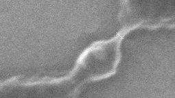
Reaction Mechanism反應機制
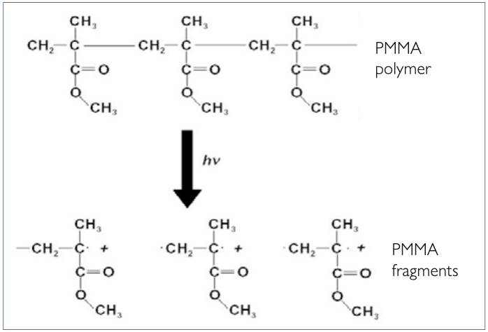
Upon electron irradiation of PMMA resists, the main chain is cleaved and the molecular mass drops from initially 950 000 g/mol (950K) to 5.000 – 10.000 g/mol. This main chain scission is primarily due to radical processes (see figure below). At an optimal dose, radicals recombine and form molecules with a molecular mass of about 5 000 g/mol. If however the dose is drastically increased, a large number of radicals are produced and undergo crosslinking so that molecules with higher molecular masses are obtained. The PMMA is turned into a negative resist. This effect is depicted in the diagram on the right which shows the gradation curve of a standard process (AR-P 671.05, 490 nm film thickness, 30 kV, developer AR 600-56). High exposure doses convert the resist into a negative resist. PMMA聚合物在電子束照射下主鏈斷裂,分子量從原來950,000 g/mol(950k)降為5,000 – 10,000 g/mol. 這種主鏈斷健主要來自於根基反應. (如左下圖). 在適合的曝光劑量下,自由基重組形成分子量約5,000g/mol的聚合物. 然而,大量提高曝光劑量,產生的大量自由基會形成架橋反應,分子量提高,反而變成負型阻劑. 右下圖顯示在標準製程(AR-P 671.05, 490nm film thickness, 30kV, developer AR 600-56), 高曝光劑量使阻劑轉為負型.
Depolymerisation opon exposure
The main chain of the PMMA is cleaved into many radical fragments
Gradation curve PMMA
Gradation curve up to maximum dose
Dose versus acceleration voltage
The sensitivity of a PMMA resist (AR-P 671.05) strongly depends on the acceleration voltage. At 100 kV a major part of the energy passes the resist without any interaction and the resist is consequently less sensitive. At 5 kV however, all electrons are absorbed. PMMA阻劑,的敏感度與加速電壓有直接關係,左圖以AR 671.05為例, 在100kV曝光參數下,能量直接穿透阻劑而無反應,敏感明顯下降. 在5kV下,所有電子都可被吸收.
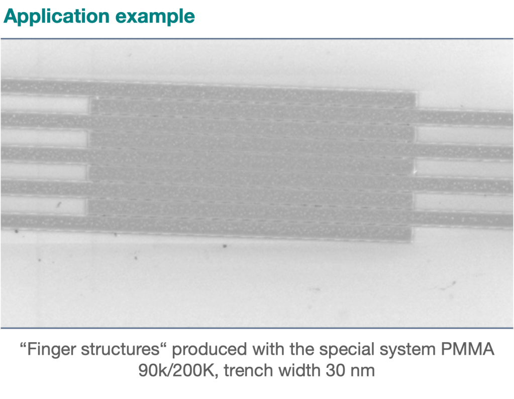
Application example
Fabrication of a PMMA bridge with AR-P 679.04 by exploiting Fresnel lenses with AR-P 671.09 the limited penetration depth at low acceleration voltage