AR-P 6200 series (CSAR 62) Copolymer positive EBL resist
Highest resolution, high contrast, for IC and mask applications

…
Product brief 產品簡介
AR-P 6200系列產品為正型電子束微影阻劑,解析度10nm,參數微調,最佳可得6nm. 調整顯影製程,可獲得較高敏感度。高對比(>15),在高膜厚應用時,深寬比可高達18。(膜厚180nm,解析度10nm).
製程穩定性高,耐電漿蝕刻(plasma etching)。
AR-P 6200系列產品主要成份為:α-甲基苯乙烯與甲基丙烯酸甲酯 共聚物 (poly(α-methylstyrene-co-methyl chloroacrylate)甲氧苯溶劑AR-P 6200屬斷鏈型阻劑。產品配方已不含光酸產生劑(photoacid generator)。產品更穩定,有效期限也更長. 目前系列產品編號有:
AR-P 6200.04
AR-P 6200.09
AR-P 6200.13
AR-P 6200.18
本產品原廠為德國ALLRESIST GmBH. 瀏覽原廠產品網頁請按原廠標識。
Click logo to link to ALLRESIST CSAR 62 product page

…
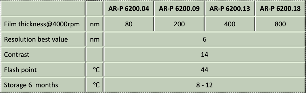
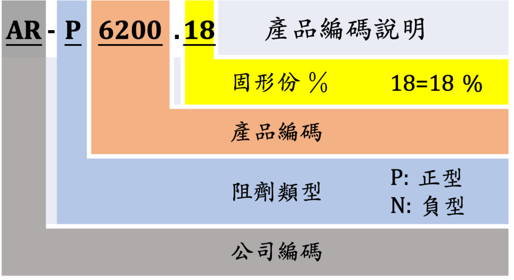
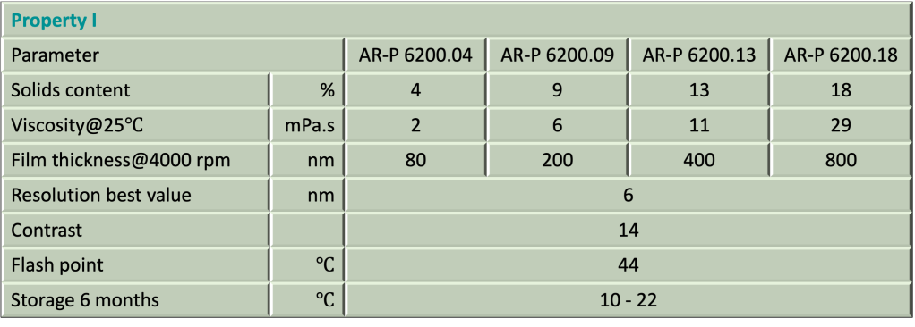
Product series & Code 產品比較及編碼說明
AR-P 6200系列產品及編碼說明如下表:
…
Product Packing & Shipping 產品包裝與出貨
Packing 產品包裝:
✅ 100 ml/瓶
✅ 250 ml/瓶
✅ 1 L/瓶
其它包裝可依客戶需求增加.
Shipping 出貨:
✅ 2 – 4 週: 徳國運出
❎ 1 週: 國內庫存
(目前暫無國內庫存)
…
Product Features 產品特性
- e-beam resist, layer thickness. 0,05-1,6 μm (6000-1000 rpm)
電子束微影阻劑,厚度範圍: 0.05-1.6 um@6000-1000rpm - high sensitivity which can be adjusted via the developer
敏感度高,可透過顯影劑調整 - highest resolution (< 10 nm) and very high contrast
解析度高(<10nm). 對比高 (14) - highly process-stable, high plasma etching resistance
製程穩定性良好. 耐電漿蝕刻
- easy fabrication of lift-off structures
lift-off 結構,製程簡單 - poly(α-methyl styrene-co-α-chloroacrylate methylester)
共聚物高分子 α-甲基苯乙烯與甲基丙烯酸甲酯 - Safer Solvent Anisole
安全溶劑(anisole)
…
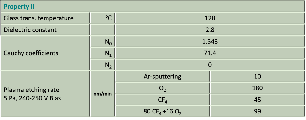
Product Properties 產品物性
…
Spin Curve 塗佈曲線

…
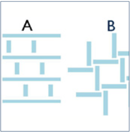
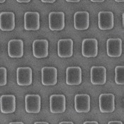
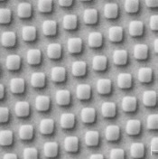
Resist Structure and Resolution 結構解析度
Structure resolution
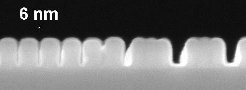
AR-P 6200.04
Resolution of up to 6 nm at film thickness of 80 nm
Resist structure
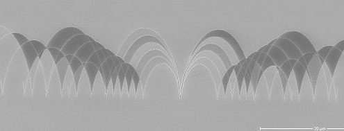
AR-P 6200.09
25-nm structures, film thickness of 180 nm, artwork
| Process Parameters | |
| Substrate | Si 4″ wafer |
| Soft bake | 1500℃ x 60sec/hot plate |
| Exposure | Raith Pioneer, 30kV |
| Development | AR 600-546 x 60sec @22℃ |
| v | |
| Process Chemicals | |
| Adhesion promoter | AR 300-80 new |
| Developer | AR 600-546 / AR 600-549 |
| Thinner | AR 600-02 |
| Stopper | AR 600-60 |
| Remover | AR 600-71 / AR 300-76 |
…
Comparison of plasma etching rate 耐蝕刻比較
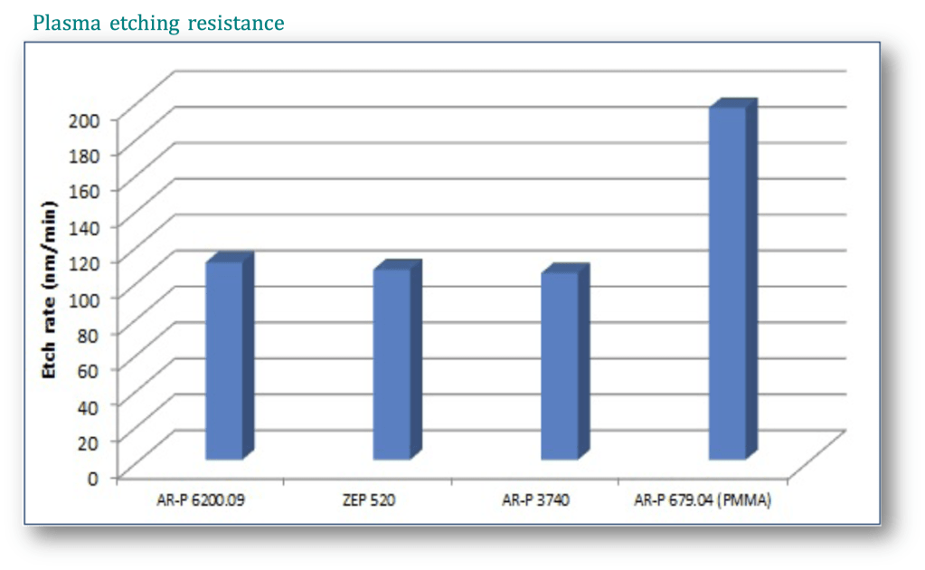
CSAR 62 is characterized by a high plasma etching resistance. In this diagram, plasma etching rates of AR-P 6200.09 are compared with those of AR-P 3740 (photoresist), AR-P 679.04 (PMMA resist) and ZEP 520A in CF4 + O2 plasma
圖為AR-P 6200.09與其它產品在CF4+O2電漿中的耐蝕刻特性.
ZXX 5xxx : 它廠共聚物EBL阻劑
AR-P 3740: 正型光阻
AR-P 679.04: PMMA 950k EBL阻劑
…
Process baseline 製程參數
| AR-P 6200.09 | |
Coating | 200 nm@4000rpm x 60 sec |
Soft bake (± 1℃) | 150℃ x 1 min hot plate, or 150℃ x 30 min convection oven |
e-Bean exposure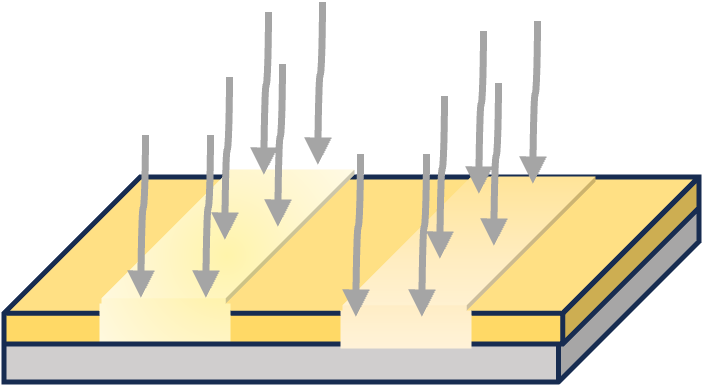 | Raith Pioneer, 30 kV Exposure dose (E0): 65 μC/cm2 |
Development (21-23±0.5℃) puddle | AR 600-546, 1 min |
Development stop and rinse | AR 600-60, 30 sec / DI water, 30 sec |
Post-bake (optional) | 130℃ x 1 min hot plate, or 130℃ x 25 min convection oven for slightly enhanced plasma etching resistance |
Customer specific technology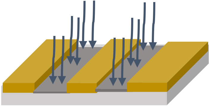 | Generation of semiconductor properties |
Resist removal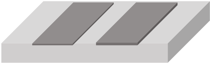 | AR 600-71, or O2 plasma ashing |
…
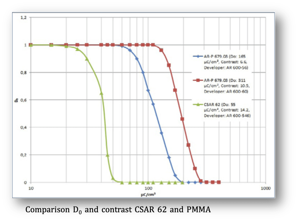
Reference for process fine tune 參數微調
e-beam exposure dose
The required e-beam exposure dose for structural imaging mainly depends on the desired minimum structure size, the developer, the acceleration voltage (1 – 100 kV), and the film thickness.
The exposure dose for AR-P 6200.09 was in this experiment (👉🏿 diagram comparison of CSAR 62 and PMMA) 55 μC/cm2 (dose to clear D0, 30 kV, 170 nm layer, developer AR 600-546, si wafer). The contrast was determined here to 14.2.
CSAR 62 is thus 3x more sensitive as compared to the standard PMMA resist AR-P 679.03 (developed in AR 600-56), or 6x more sensitive if developed in AR 600- 60. Also the contrast is higher by a factor of 2 and 1.4, respectively.
An additional increase in sensitivity due to addition of sensitivity-enhancing components occurs already during exposure. A post-exposure bake is thus not required.
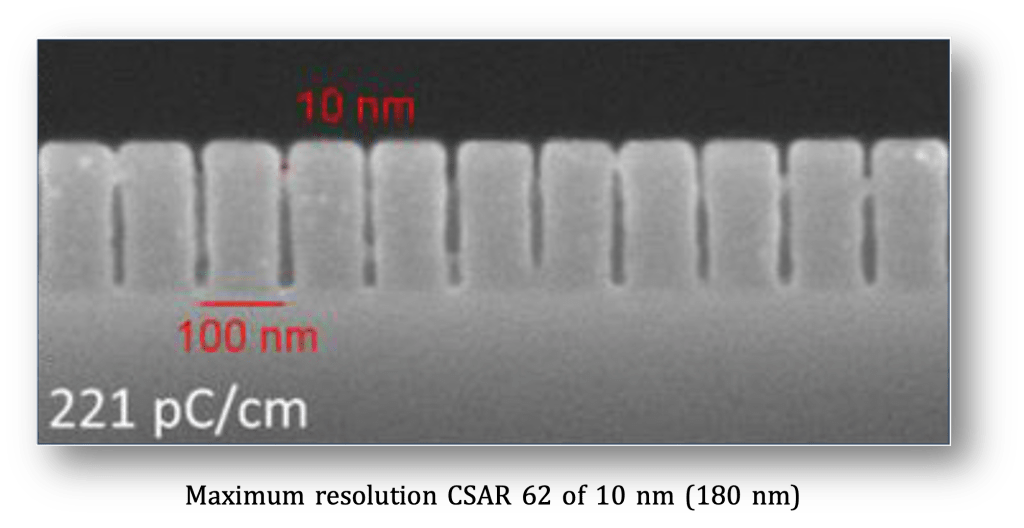
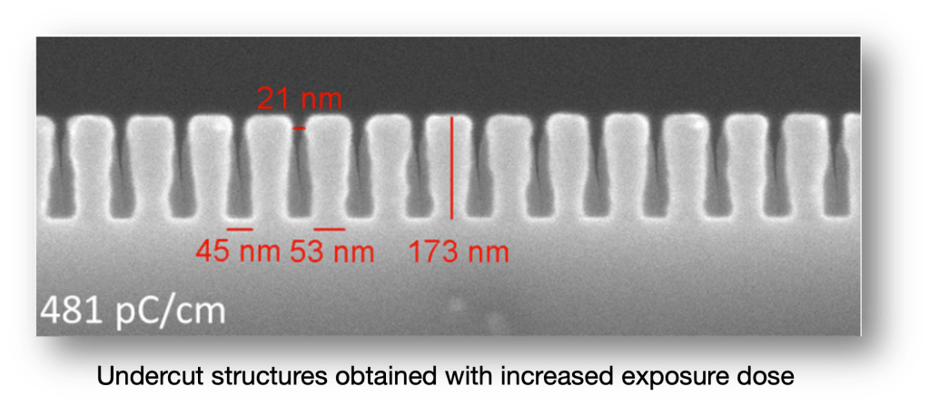
For the fabrication of 10-nm trenches (174 nm film, 100n pitch), AR 6200.09 requires a dose of approx. 220 pC/cm (30 kV, developer AR 600-546)
曝光劑量的選擇與結構,厚度,顯影劑及加速電壓(1-100kV)有關. 左下圖為AR-P 6200.09, 在矽晶圓上塗佈厚度170nm, 以30kV加速電壓,曝光劑量55uC/cm2, 顯影劑為AR 600-546. 計算對比為14.2. 相較於PMMA AR-P 679.03於顯影劑AR 600-56(對比為2), 敏感度高出3倍. 如果AR-P 679.03以AR 600-60顯影(對比為1.4),則敏感度為6倍.
配方中強化敏感度成份,於曝光後就起作用,因此並不需要曝後烤.
右下圖為AR 6200.09於矽晶圓上形成10nm寬的槽溝(厚度170nm,間距100nm),所需劑量約為220pC/cm (30kV加速電壓,AR 600-546顯影劑)
developer & development
For the development of exposed resist films, developers AR 600-546, 600-548 and 600-549 are recommended. As weaker developer, AR 600-546 provides a wider process window. If the stronger developer AR 600-548 is used, the sensitivity can be increased 6-fold to < 10 μC/cm2. The intermediate developer AR 600-549 renders the CSAR 62 twice as sensitive as compared to AR 600-546, it shows also no dark erosion and has a contrast of 4.
For immersion development, generally development times of 30 – 60 seconds are recommended. If developer AR 600-546 is used, even after 10 minutes at room temperature no erosion of unexposed areas is detected.
Developer AR 600-548 in contrast attacks resist surfaces already after two minutes visibly. If, however the development process is carried out at temperatures of approx. 0 °C, no dark erosion is observed even after 5 minutes (which is however associated with a reduction of sensitivity).
The development procedure should be stopped quickly. For this purpose, the substrate is moved for 30 seconds in stopper AR 600-60. Optionally, the substrate may there after be rinsed for 30 seconds with DI water to remove all residual solvent.
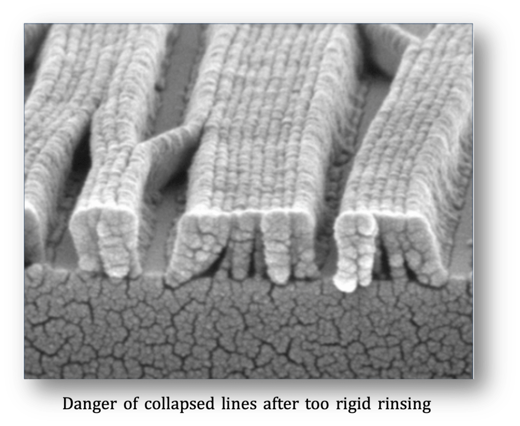
Note: Please take into account that rigid rinsing procedures may lead to a collapse of smaller structures (👉🏿see image below).
A post-bake for special working steps at max. 130 °C results in a slightly improved etching stability during wet- chemical and plasma-chemical processes.
曝光後的顯影,建議的顯影劑為AR 600-546, AR 600-548及AR 600-549. AR 600-546為較弱顯影劑,製程穩定. 使用較強顯影劑 AR 600-548,可提高敏感度至6倍(<10uC/cm2). 強度介於中間的AR 600-549,相較於AR 600-549,敏感度提高約2倍,且無顯影損失及對比為4.
浸泡式顯影通常需時30-60 sec. 使用AR 600-546在室溫下浸泡10分鐘在為曝光區域也不會有顯影損失.
強顯影劑AR 600-548則在2分鐘後就可觀察到阻劑表面受到侵蝕. 然而,在0℃低溫下顯影5分鐘後也無顯影損失現象. 但低溫下顯影,敏感度會降低.
顯影完成後需儘速停止顯影反應. 可以AR 600-60浸泡30sec抑制顯影反應,隨後再以純水洗去殘留溶劑 (30sec).
附註: 請小心潤洗程序, 可能造程細小結構的坍塌. (如下圖)
以130℃硬烤可稍微改善耐濕蝕刻及乾蝕刻性質.
lift-off structure
Resist CSAR 62 is well suited to generate lift-off structures with a resolution of up to 10 nm. If the dose is increased by a factor of 1.5 – 2, narrow trenches with defined undercut can be fabricated with AR-P 6200.09.
CSAR 62非常識合於浮剝離結構(lift-off), 解析度可達10nm. 以AR 6200.09為例,曝光劑量提高1.5 – 2倍, 細槽溝也可形成下切型結構.
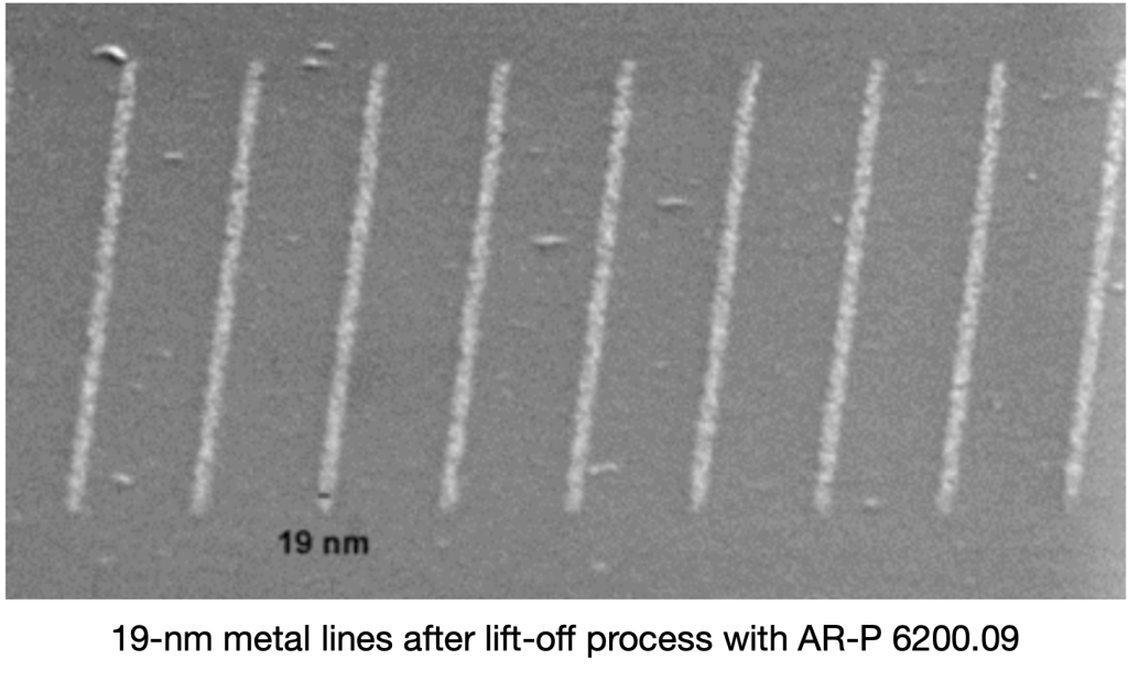
After vapor-deposition of metal and subsequent easy lift-off, metal structures remain
金屬蒸鍍,浮剝離後留下的金屬結構
high film thickness application
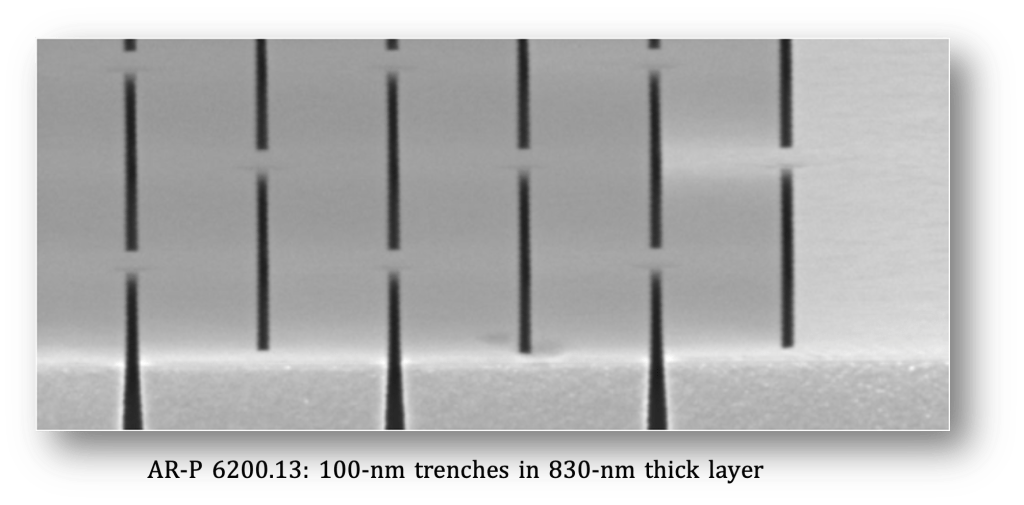
Films with a thickness of up to 800 nm can be produced With AR-P 6200.13, and even 1.5-μm films are possible with experimental sample SX AR-P 6200/10.
AR-P 6200.13厚度可達800nm. SX AR-P 6200/10 (AR-P 6200.18)厚度達1.5um)

CSAR 62 is also applied in various two-layer systems and can be used both as bottom and as top resist.
於雙層結構應用,可當頂層或底層阻劑

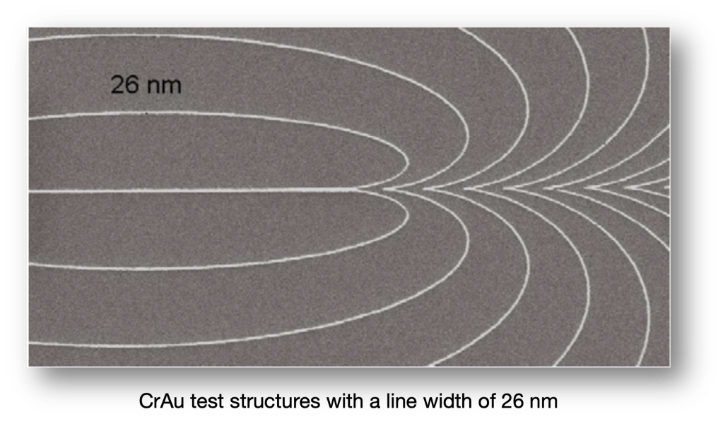
At a film thickness of 380 nm, 100-nm lines and spaces can be obtained on a chrome mask with AR-P 6200.13. The sensitivity is 12 μC/cm2 (20 kV, AR 600-548).
Another field of application for CSAR 62 is the production of mask blanks which are coated with our resist and offered by our partners:
於空白光罩應用(mask blanks)
Application examples 應用實例
Circuits for the 5 GHz range which are primarily needed for wireless Bluetooth or Wi-Fi technologies can in future be produced with CSAR 62. E-beam lithography is also required for the research on nanomaterials like graphene, for three-dimensional integrated circuits as well as for optical and quantum computers. The computing power or memory density is constantly increased in each of these technologies. Applications with the highest demands on computing power (supercomputers), e.g., in computational fluid dynamics or in space applications, thus also demand microchips with highest integration density.
CSAR 62電子束微影應用範圍廣汎,例如未來5G的無線通訊電路製作,石墨烯等奈米材料的研發, 3D積體電路,光學及量子電腦等等. 這些科技的運算速度及記憶體密度不斷增加. 需要高速運算的應用, 例如計算流體力學,或太空科技的超級電腦都需要高速運算及高密度晶片
mask blanks
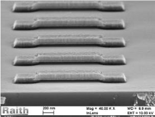
Experts at the HHI Berlin have already tested CSAR 62 on mask blanks (👉Fig. 1). They immediately achieved a resolution of 50 nm which is an excellent value for masks. To date, 100 nm lines and above are used on masks. Currently test coatings of mask blanks with CSAR 62 are con- ducted, and samples will be offered by our partners to all customers in the near future.
CSAR 2014年開發成功時,位於柏林的電信研究所(Fraunhofer HHI)成功的測試於空白光罩,解析度達50nm(如下圖1), 相較於當時僅100um,表現相當優異.
Fig. 1 CSAR 62 test structure on a mask blank with 50 nm lines and 50 nm trenches; pitch line & space here 99.57 nm
high resolution lithography
In the work group for nanostructured materials of the MLU Halle, CSAR 62 is mainly used in highest-resolution lithography for the lift-off and as etching mask for dry chemical etching processes. The new resist offers several specific advantages. It achieves the high resolution of PMMA, but at a much lower dose. Due to the high contrast, vertical resist edges are generated which allow a reliable lift-off even with thinner films and ensure a uniform lift-off up to 20 nm:
德國MLU Halle(大學)的奈米結構材料研究小組將CSAR 62主要用於乾蝕刻製成需要的高解析度浮剝離阻劑. 此新型阻劑提供的優點包括:
低曝光劑量. 相較於高解析度PMMA阻劑, CSAR 62曝光劑量低很多.
高對比度,可型成垂直邊緣結構. 此優點在低膜厚阻劑仍可維持穩定的懸剝離製程. 如圖20nm寬的金屬懸剝離製程


The goal in the lift-off of metal structures is however not always to go beyond the limits of resolution. Typical applications for example in the contacting of nanowires rather require dimensions in a range of 30-50 nm, which can also be realized with other resists. The „resolution reserve“ of CSAR 62 however allows for significantly improved structure accuracy and faster design with less iteration.
使用懸浮剝離製程的金屬結構,不見得都需要用到高解析度的阻劑: 像奈米線ㄧ般介於30-50nm, 其它阻劑也可達到. CSAR 62的解析度優點還可改善結構的精確性,更不用談其加速產品的設計流程的優勢.
During dry chemical etching, for example in the structuring of silicon nitride, CSAR combines the best of two worlds: It not only allows the use as a high-resolution positive resist similar to PMMA, but also offers a stability which is comparable to novolacs.
This facilitates the production of pattern with sharp edges that provide the required etch stability without the disturbing faceting at the edges which otherwise occurs frequently. CSAR 62 is normally used for films with thickness values between 50 and 300 nm. Intense plasma etching for the fabrication of deep etch structures however requires significantly thicker resist layers and places special demands on resolution and contrast. Resist AR-P 6200.18 was thus designed for high layer thicknesses of 0.6-1.6 μm and is particularly well suited for the realization of high metal structures with lift-off, deep plasma etching processes or nanowires.
在乾蝕刻的製程,例如氮化矽的圖案,CSAR62同時具有如PMMA阻劑的高解析度,及酚醛系的安定性. 這特性使圖案邊緣明確,,提高蝕刻的穩定性.
CSAR 62通常用於膜厚50 – 300 nm之間. 但高深度結構的高強度電漿蝕刻需高厚度阻劑同時具備高解析度及高對比等特性.
AR-P 6200.18厚度範圍0.6 – 1.6 um,非常適合高厚度金屬的懸浮剝離(如右圖5), 深乾時刻及奈米線等製程.

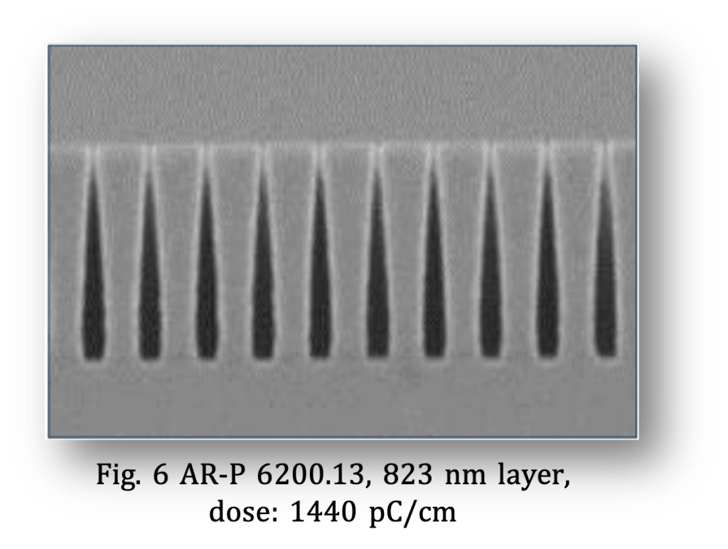
It is nonetheless possible to produce trenches with a width of < 100 nm at a film thickness of 800 nm. The high contrast is made possible through the use of our developer AR 600-546. By increasing the irradiation dose, the degree of the generated undercut can be adjusted specifically (Fig. 5 +6). Each user can thus select the most favorable profile for his specific lift-off process.
高對比及專用顯影劑AR 600-546,使得在800nm膜厚形成<100nm的溝槽仍然是沒有問題. 下切結構可依曝光強度加以調整(圖5+6), 使用者可依需求選擇最適合參數.
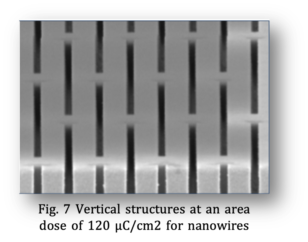
If circles are irradiated and developed in such thick layers, columns (nanowires) can be produced due to a high metal deposition (evaporation, sputtering or electroplating) (see vertical edges in Fig. 7).
如果在高膜厚可形成圖案,金屬高柱可直接以蒸鍍,濺鍍,電鍍等方法沉積. (圖7)
2-layer lift-off for L-shaped structure
The task in the IAP of the Friedrich Schiller University of Jena was to produce very small, high-precision rectangular structures. For this purpose, a two-layer system composed of AR-P 6200.09 as top layer and AR-P 617.06 as bottom layer was established. After exposure with e-beam writer Vistec SB 350OS, CSAR 62 was patterned with developer AR 600-546. The bottom layer was subsequently developed with developer AR 600-55, followed by coating with gold. The lift-off was performed with a mixture of acetone and isopropanole. The resulting structures are shown in Fig. 12. The structure sizes are 38 nm with structure intervals of approximately 40 nm. In particular to be regarded positively are the small radii of curvature at the corner of the inside of the „L“.
應用光子實驗室(位於Jena的Friedrich Schiller大學)有一實驗需非常高精密小尺寸的長方形結構. 採用由AR 6200.09(頂層)及AR 617.06(底層)的雙層阻劑. 以電子束設備 (Vistec SB 350OS)曝光. 再以AR 600-546顯影頂層AR 6200.09, 隨後以AR 600-55顯影底層AR-P 617.06. 完成再沈積金層. 以丙酮及異丙醇混合液進行懸浮剝離. 結果如下圖12所示. 金屬結構寬約38nm, 結構間距約40nm. 特別一題的是L形可形成接近直角的結構.
Fig. 12 High-precision L-shaped structures, produced with the two-layer system
AR-P 6200.09 / AR-P 617.06; right 2 Layer systems

high precision square structures
A similar objective was pursued by this working group with respect to the fabrication of square structures. The aim was again to obtain corners with particularly high resolution. For this purpose, a CSAR 62 film with a thickness of 100 nm was irradiated with 50 kV and developed with developer AR 600-546. In addition to the excellent properties of CSAR 62, also the irradiation design is of vital importance (see Fig. 13, centre: A; right: B).
應用光子實驗室(位於Jena的Friedrich Schiller大學)另有一類似實驗需方形圖案. 目標一樣要獲得高解析度的方形轉角結構. CSAR 62在膜厚100nm,以50kV加速電壓曝光,再以AR 600-546顯影. 如圖13所示, 除了阻劑特性外,曝光程序一樣重要.
Fig. 13 Different irradiation designs and resulting square structures (centre: A; right: B)
low temperature development
The sensitivity of CSAR 62 is strongly influenced by the choice of the developer. In comparison to the standard developer AR 600-546, the sensitivity can almost be increased tenfold if AR600-548 is used which is however accompanied by an incipient erosion of unexposed resist areas. This is tolerable to a certain extent: If, for example, always 10% of the layer is lost, can this effect be compensated for in advance. Erosion can also be avoided if the development is carried out at lower temperatures, but this is again associated with a certain loss of the previously gained sensitivity. It thus comes down to the fact that an optimization of the process is required. The lower temperatures offer, due to the gentler development step, the possibility to increase the contrast or reduce the edge roughness.
顯影劑對CSAR 62的敏感度影響很大. 使用AR 600-546顯影劑,相較於AR 600-548,敏感度可增加10倍.
用AR 600-548會有顯影損失. 一致性的顯影損失,例如10%的膜厚損失,可以事先補償,不會影響太大. 顯影損失也可以低溫顯影加以避免,但是敏感度還是較低.
因此製程參數依需要調整是必要的. 顯影溫度越低,顯影反應越平和,可增加對比及降低結構邊緣的表面粗糙度.
Fig. 14-16 show the sensitivities and resolutions of AR-P 6200.04 at 6 °C and 21 °C (room temperature). Due to the high contrast at 6 °C, a resolution of 6 nm could be achieved.
下圖14-16顯示AR-P 6200.04在6℃及21℃顯影的敏感度與解析度. 由於在低溫顯影的高對比性, 6nm的解析度可於6℃顯影調件下獲得.
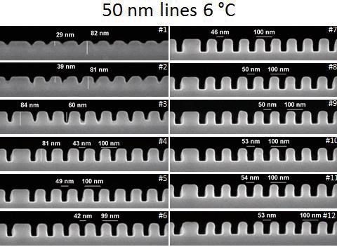
Fig. 14 CSAR 62 structures at 6 °C, opt. dose 195 pC/cm
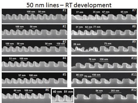
Fig. 15 CSAR 62 structures at 21 °C, opt. dose 121 pC/cm
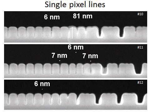
Fig. 16 Max. resolution of 6 nm at 235 pC/cm and 6 °C
nano structures written at 100kV
At the Karlsruhe Institute of Technology, the suitability of CSAR 62 for the fabrication of complex architectures was investigated in detail. CSAR 62 layers were irradiated with e-beam writer EBPG5200Z at 100 kV and developed with developer AR 600-546. The results are shown in the figures below.
Karlsruhe理工學院詳細研究CSAR 62在複雜結構的適用性. 下圖為100kV加速電壓(EBPG5200Z)AR 600-546顯影結果.
Fig. 17 SEM images (gold-sputtered): CSAR 62 nanostructures, parameters: film thickness 200 nm, dose 225 μC/cm2, 100 kV, developer AR 600-546, 3 min,stopper AR 600-60


A particular challenge is the writing and development of nano-sized hole structures. Using CSAR 62, a diameter of remarkable 67 nm could be realized, whereby the sophisticated structural element shows a very regular pattern
比較困難的是形成孔眼圖案,右上圖是以CSAR 62寫出直徑67nm的圓孔
T-gate application with AR-P 617
Developer for T-gate applications with AR-P 617:
X AR 600-50/2 is a new, sensitive and highly selective developer for high-tempered AR-P 617 layers (SB>180 °C). PMMA or CSAR 62 layers are not attacked, which is of particular importance for multilayer processes e.g., in the manufacture of T-gates.
顯影劑X AR 600-50/2是高選擇性及感度新顯影劑,適用於高溫軟烤(>180℃)的AR-P 617阻劑. 但確不會攻擊PMMA或CSAR 62等阻劑.可用於製作T-gate的多層製程.
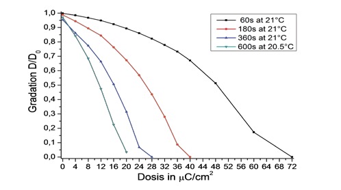
Fig. 18 AR-P 617, film thickness: ~1 μm, SB 10 minutes at 200 °C, 50 kV, dose variations, dependence of the sensitivity on the development time with developer X AR 600-50/2 at room temperature, stopper AR 600-60
The sensitivity can easily be controlled via the duration of the development. At a development time of 60 s, the dose to clear is about 70 μC/cm2, after 3 minutes of development about 40 μC/cm2, after 6 minutes 25 μC/cm2, and after 10 minutes about 20 μC/cm2! The amount of dark erosion is very low, even at longer development times
敏感度可透過顯影時間控制. 60 sec顯影時間,最低劑量約為70uC/cm2. 3分鐘顯影,最低劑量約為約為40uC/cm2. 6分鐘為25uC/cm2. 10分鐘則降至約為20uC/cm2. 在長顯影時間可維持相當低的顯影損失.
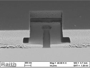
3D-resist profile after development and prior to the metallization step

T-gate after lift-off
Metal bridge structures
fluorescent film
Fluorescent dyes can be embedded into positive-tone e- beam resists like CSAR 62 and PMMA. For this purpose, both PMMA and CSAR 62 polymers were prepared in a solvent mixture which also dissolves the fluorescent dyes to a sufficient extent. The use of different fluorescent dyes allows a defined adjustable emission in various wavelength ranges. These dyes are highly process-stable, and structu- ring is performed in the same manner as in corresponding standard processes with uncoloured e-beam resists. By embedding dyes into CSAR 62, resist films could be ge- nerated which optionally show violet, blue, yellow, orange or red fluorescence. The intense fluorescence is retained even after tempering at 180 °C.
電子束微影阻劑例如CSAR 62及PMMA可參雜螢光染料. 配製方法是於含有足量染料溶劑混液中加入PMMA或CSAR 62高分子. 使用不同螢光染料可調整其發光波長範圍. 添加染料為穩定的製程,加入染料的阻劑可維持原來的製程參數. 發光顏色包括紫色,藍色,黃色,橘色及紅色等螢光. 阻劑經烘烤達180℃,螢光強度可維持.
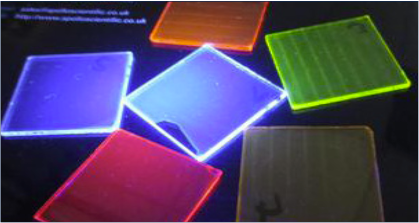
Intensely fluorescing films of CSAR 62 on glass
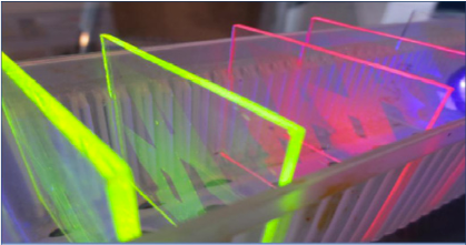
Fluorescent structures (UV irradiation with a wavelength < 250 nm, developer AR 600-546)
Fluorescent PMMA architectures were produced by Precision Optics Gera GmbH via electron beam lithography. These structures could be developed residue-free using an optimized developer. If these resist structures are excited with UV light (as shown in the two pictures), they begin to glow intensely.
德國光學公司(Precision Optics Gera GmbH)使用電子束微影技術生產元件. 使用適合的顯影液可顯影完全,不殘留. 如下圖所示,含螢光染料的阻劑結構.
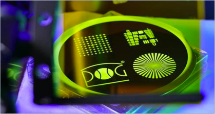
Yellow fluorescent PMMA-based resist architectures

Red fluorescent PMMA-based resist architectures
Due to the properties of these e-beam resists, resolutions up to the 10 – 20 nm range are possible. The main field of this application is in optical industry; these materials are e.g., required for night vision devices. Fluorescent resist films are furthermore used for applications in microscopy.
電子束微影阻劑的解析度可達10-20nm, 這方面的應用主要在光學工業,例如夜視元件. 另外也可於顯微鏡方面的應用.
…
Contents are base on ALLRESIST product TDS.
Click logo below to link to ALLRESIST CSAR 62 product page .
內容取材自原廠產品技術資料,連結原廠請按下方標識。

