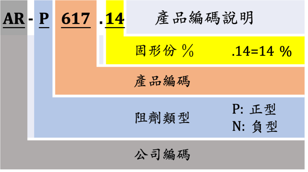
AR-P 617 Series Positive Co-polymer e-Beam Resist
for nanometer lithography, highest resolution, Copolymer 33% MA
…
Product Brief 產品簡介
AR-P 617 系列產品高分子是MMA(甲基丙烯酸甲酯)與MA(甲基丙烯酸)共聚物 poly(MMA-co-MA, MA 33%).溶劑為PGME. 產品為正型阻劑,適合各種電子束微影製程, 應用於光罩製作,積體電路等高精密圖案製程(multilayer & planarization),對玻 璃, 矽晶元,金屬等,有良好的接著性.
此系列產品過慮規格為0.2um.
由於共聚物及組合成份的化學特性,其敏感性(sensitivity)是PMMA阻劑的3-4倍. 同時其對比性(contrast)也優於PMMA阻劑. 顯影後的阻劑結構在240°C能有良好的安定性.(thermal-stability).
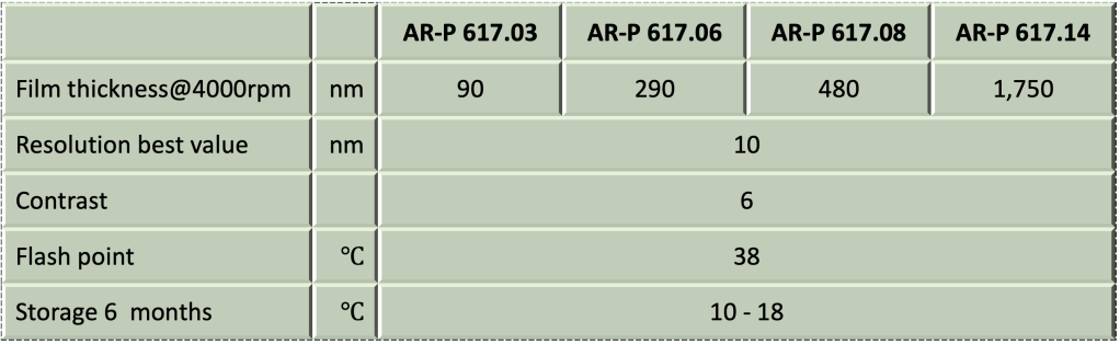
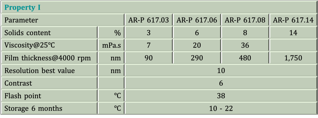
系列產品,最低固型份含量, 可降低膜厚到30nm. 適合奈米等級微影.
目前系列產品有:
AR-P 617.03
AR-P 617.06
AR-P 617.08
AR-P 617.14
…
Product Code & Comparison 產品編碼及比較
…
Product Packing & Shipping 產品包裝與出貨
Packing 產品包裝:
✅ 250 ml/瓶
✅ 1 L/瓶
其它包裝可依客戶需求增加.
Shipping 出貨:
✅ 2 – 4 週: 徳國運出
❎ 1 週: 國內庫存
(目前暫無國內庫存)
…
Product Features 產品特性
- e-beam, deep UV (248 nm)
適合電子束微影, 深紫外線(248 nm) - highest resolution, high contrast
高解析度(10nm), 高對比. - strong adhesion to glass, silicon and metals
對玻璃, 矽及金屬等基材有良好的接著性 - 3-4 times more sensitive than PMMA
相較於PMMA阻劑, 敏感度可高出3-4倍 - sensitivity can be adjusted via the soft-bake
敏感性能可透過軟考(soft-bake)調整 - for planarization and multi-layer processes
應用於平坦化及立體結構積層電路 - temperature-stable up to 240 °C
耐溫240°C - copolymer on the basis of methyl methacrylate and methacrylic acid.
高分子為甲基丙烯酸甲酯與甲基丙烯酸共聚物poly(MMA-co-MA) - safer solvent 1-methoxy-2-propanol
使用安全溶劑丙二醇甲醚 (PGME-Propylene glycol methyl ether)
…
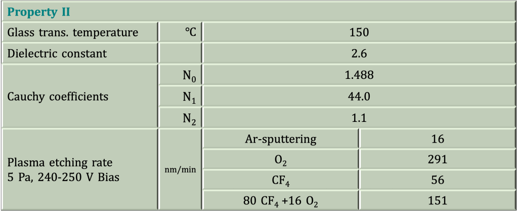
Product Properties 產品物性
…
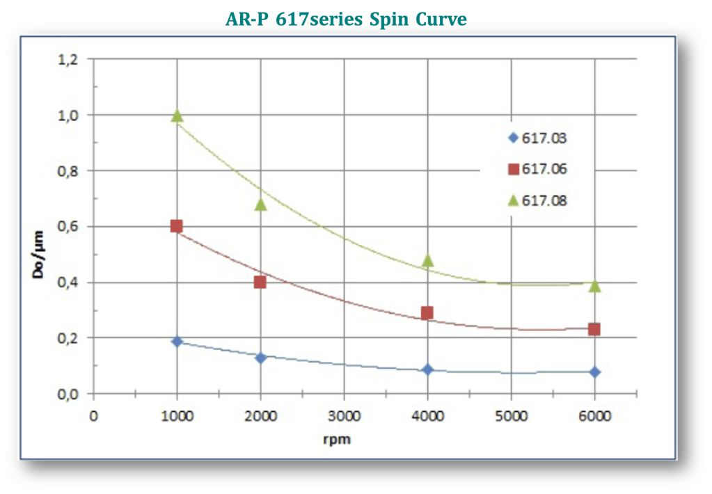
Spin Curve 塗佈曲線
…
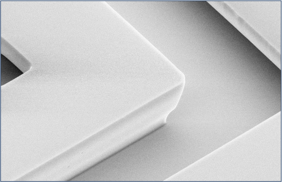
Resist Structure and Resolution 結構解析度
Structure resolution
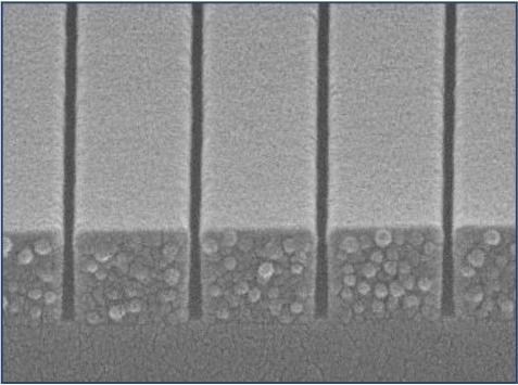
AR-P 617.03
30 nm trenches at film thickness of 120 nm
Resist structure

AR-P 617.03
150 nm lines across 200 nm oxide steps
…
Process baseline 製程參數
This diagram shows exemplary process steps for resists of AR-P 617series. All specifications are guideline values which must be adapted to own specific conditions. For further information on processing, 👉“Detailed instructions for optimum processing of e-beam resists”. For recommendations on wastewater treatment and general safety instructions, 👉”General product information on Allresist e-beam resists”.
圖示AR-P 617.06產品製程參數的範例. 所有參數為參考值,使用者應依設備環境實際狀況加以調整
| AR-P 617.06 | |
Coating | 290 nm@4000 rpm x 60 sec |
Soft bake (±1℃)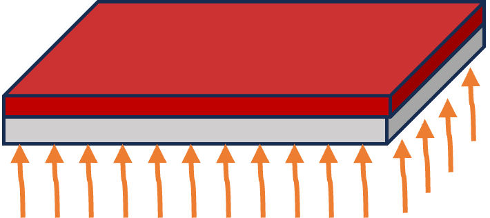 | 200℃ x 25 min/hot plate, or |
| 200℃ x 60 min/convection oven | |
| e-Beam exposure dose (E0) 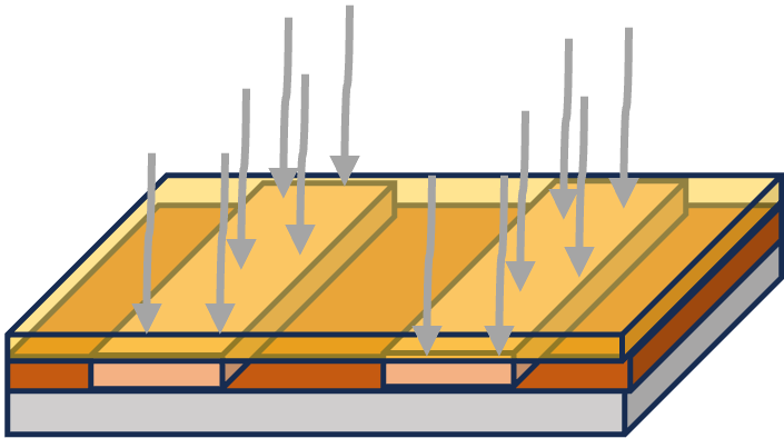 | ZBA 21, 20 kV |
| Exposure dose (E0): 30uC/cm2, L/S=500nm | |
| Development (21-23±1℃) puddle 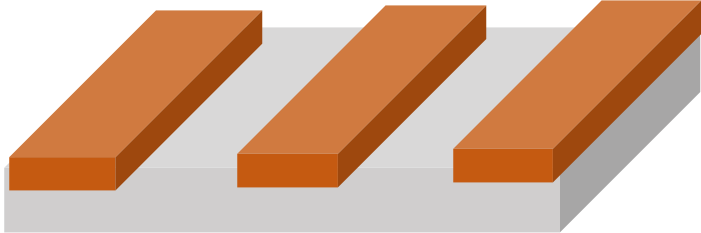 | AR 600-50 60 sec |
| Stopping | AR 600-60 30 sec |
| Post-bake (optional)  | 130℃ x 1 min/hot plate, or 130℃ x 25 min/convection oven for slightly enhanced plasma etching resistance |
| Customer specific technology 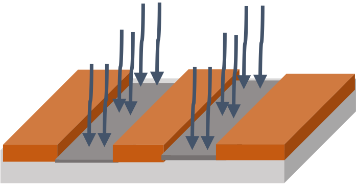 | Generation of semiconductor properties |
Removal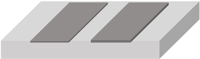 | AR 300-76, or O2 plasma ashing |
…
Relationship of film thickness, solid content and spin speed

…
2-layer Under-cut for Lift-off Processing instructions
The sensitivity of the resist increases with increasing softbake temperature due to the more intense formation of anhydrides of the methacrylic acid under separation of water (👉diagram dose vs. softbake temperature). AR-P 617 tempered at 200 °C is therefore about 20 % more sensitive as compared to a tempering at 180 °C. The dose can be adjusted accordingly, which is of major importance for two-layer systems with two layers of AR-P 617. In this case, at first the bottom layer is dried at 200 °C and then tempered at 180 °C together with the upper film.
Due to differentiation processes, the lower layer is attacked faster by the developer and pronounced undercut structures are formed (lift-off). These lift-off structures can also be produced with the two-layer system PMMA/copolymer. At first AR-P 617 is coated and tempered at 190 °C, then the PMMA resist AR-P 679.03 is applied by spin-coating and dried at 150 °C. After exposure, both layers are developed in one step e.g. with AR 600-56, treated with stopper AR 600-60 and rinsed.
阻劑共聚物中相鄰的甲基丙烯酸(methacrylic acid)在軟考溫度增加時因脫水反應更容易形成酸酐,(如圖曝光劑量與軟烤溫度). AR-P 617的敏感度在200℃軟烤溫度比180℃高出20%. 曝光劑量可依此調整,這在雙層結構中是很重要的參數. 一般程序是第一層先以200℃軟烤, 塗佈第二層後再以180℃同時對兩層阻劑軟烤. 顯影劑對第一層反應較快因而形成下切型結構適合懸浮剝離製程(左下圖). 也可採用PMMA/AR-617雙層結構. AR-P 617.06先以190℃軟烤,塗佈PMMA AR-P 679.06後以150℃軟烤. 雙層阻劑曝光後以AR 600-56顯影(右下圖).
Lift-off structure with two layers of AR-P 617
After development with AR 600-50
Bottom: AR-P 617.06, 400 nm thick, tempered at 200 °C
Top: AR-P 617.06, 500 nm thick, tempered at 180 °C
Undercut structure with PMMA/copolymer
Two-layer system PMMA/copolymer after development
Bottom: AR-P 617.06, 400 nm thick, tempered at 190 °C
Top: AR-P 679.06, 180 nm thick, tempered at 150 °C
Dose vs. softbake temperature for AR-P 617
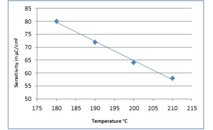
With increasing temperature, the sensitivity of AR-P 617.08 (film thickness 680 nm) increases linearly.
Gradation curve of AR-P 617
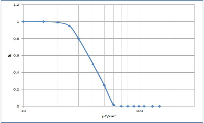
At a film thickness of 350 nm, a contrast of 5.0 was determined (30 kV, developer AR 600-50)
…
Sensitivity-enhancing reaction during tempering
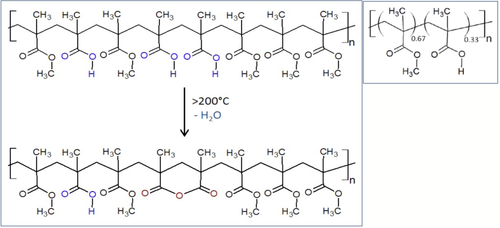
The copolymer composed of methyl methacrylate and methacrylic acid is, in contrast to pure PMMA products, able to form a 6-ring during thermal loading. In this case, 2 methacrylic acid groups have to be arranged adjacent to each other in the polymer chain (see large structural formula left), which statistically occurs with sufficiently high frequency at a mixing ratio of 2 : 1 (see molecular formula top right). The reaction is possible at this temperature, since the water which is produced during the reaction is a very good leaving group.The 6-ring which is formed breaks apart more easily during irradiation with electrons than the aliphatic chain remainder which causes the higher sensitivity of the copolymer. Once adjusted, the sensitivity will remain unchanged. The reverse ring-opening reaction is impossible.
不同於的PMMA反應機制,AR-P 617共聚物(甲基丙烯酸甲酯與甲基丙烯酸)可在軟烤溫度下形成6環結構. 在分子鏈中必需有兩個相鄰的甲基丙烯酸才能形成6環的結構(如上左圖). 統計分析, MMA與MA比例約2:1最適合. (如上右圖).
水是在此溫度下產生的離去基團.
此共聚物阻劑有較高的敏感度主要來自於分子鏈中的6環比起脂肪鏈更易於電子束下斷鍵. 因不會有反向的開環聚合反應,參數調整確定後,阻劑敏感度可維持穩定.
…
Planarization with AR-P 617 平坦化應用範例
Due to the excellent coating properties is it possible to level out topologies which are present on the wafer before development. In this example, 200 nm high oxide structures were coated with AR-P 617.08. The film thickness was 780 nm. After exposure (20 kV) and development (AR 600-50, 2 min), the structured wafer is covered with entirely planar resist lines.
AR-P 617系列有良好的塗佈特性,對基板已有的高低結構不影響其平坦化效果.
左圖範例為200nm高的氧化矽上塗佈780nm厚的AR-P 617.08.
以20kV電子束曝光, 顯影(AR 600-50, 2 min).
在有高低氧化矽結構表面佈滿平坦的阻劑線.
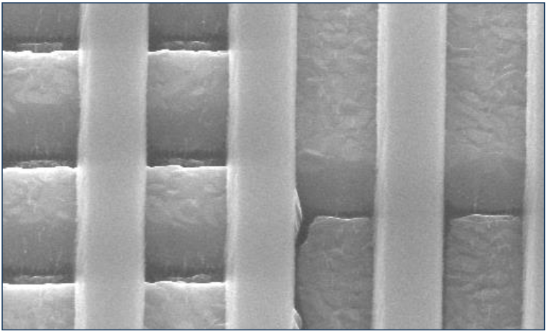
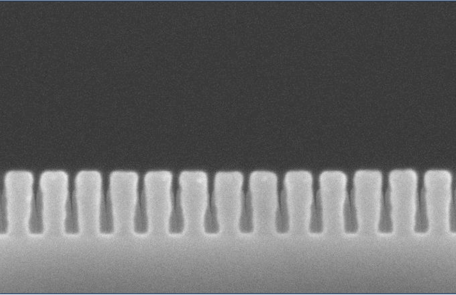
AR-P 617.12 Structures across topologies
…
