AR-N 7700 series negative CAR type e-beam lithography resist
High resolution resist with steep gradation for semiconductor process
…
Product brief 產品簡介
AR-N 7700系列, 為化學放大 chemically amplified (CAR)負型電子束微影阻劑 (negative tone EBL resist). 可在電子束及深紫外線(deep UV)曝光, 對比度高,適合於各類半導體製程. 產品系列目前有:
AR-N 7700.08
AR-N 7700.18
…
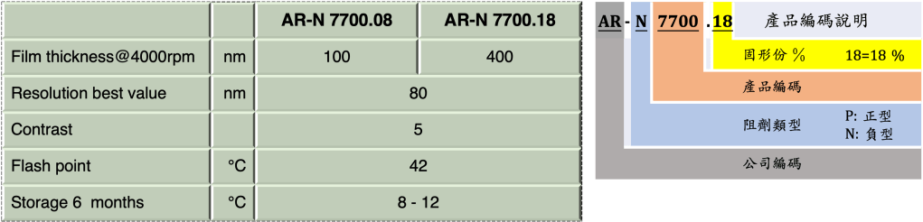
Product series & Code 產品比較及編碼說明:
…
Packing 產品包裝:
✅ 250 ml /瓶
✅ 1 L /瓶
其它包裝可依客戶需求增加.
Shipping 出貨:
本產品未列固定生產排程,交期與報價需先詢問。估計交期為:
✅ 4 – 8 週. 徳國運出
…
Product Features 產品特性
- e-beam, deep UV; chemically enhanced (CAR)
化學放大型阻劑,曝光源可為電子束, 深紫外線 - high contrast for digital reproduction with excellent sensitivity
高對比度, 高敏感度 - negative-tone with high resolution in the UV range 248-265 nm and 290-330 nm
在紫外線波長248 – 265 nm及290 – 330nm下曝光為負型模式
- plasma etching resistant, temperature stable up to 140 °C
耐乾蝕刻, 高溫穩性定達140℃ - novolac, acid generator, cross-linking agent
主要成份含酚醛樹酯, 光酸產生劑,架橋劑等 - safer solvent PGMEA
溶劑使用較安全的丙二醇甲醚醋酸酯
…
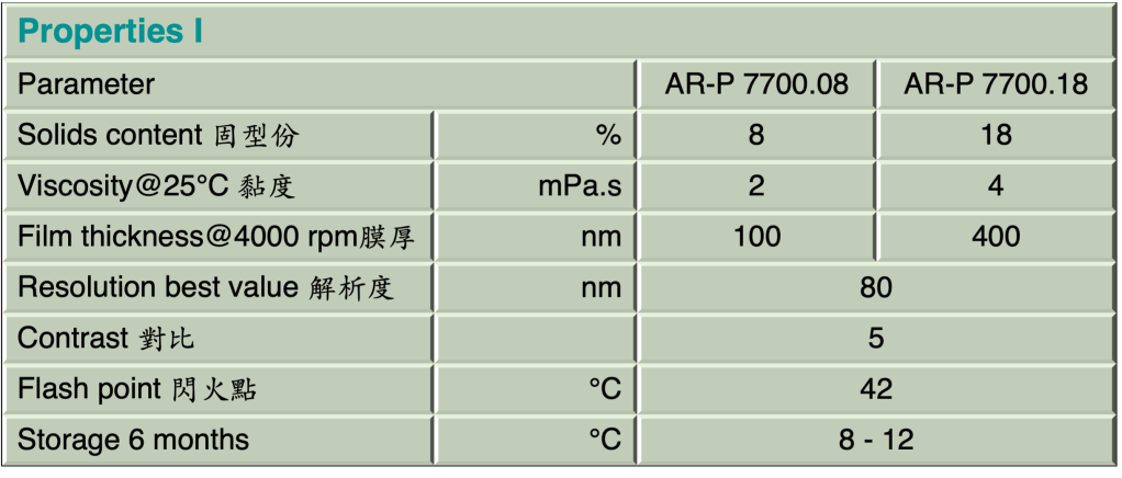
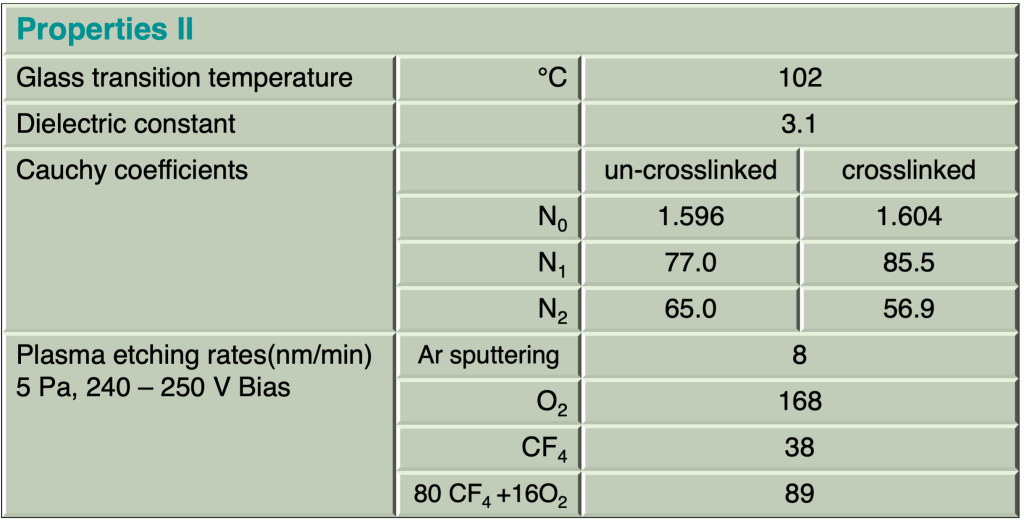
Product Properties 產品物性
…
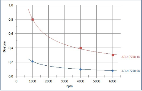
Spin curve 塗佈曲線
…
Structure resolution
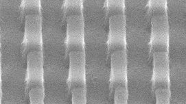
AR-N 7700.18 112 x 164 squares, film thickness of 400 nm
Resist structures
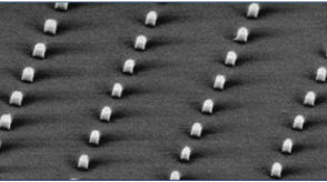
AR-N 7700 500-nm dots, written with a dose of 12 μC/cm2 (30 kV).
Process parameters
| Substrate | 4″ Si wafer |
| Soft bake | 85℃x90sec, hot plate |
| Exposure | ZBA 21, 30kV |
| Development | AR 300-46, 60sec 22℃ |
…
Process baseline 製程參數
This diagram shows exemplary process steps for AR-N 7700 resists. All specifications are guideline values which have
to be adapted to own specific conditions. For further information on processing, 👉“Detailed instructions for optimum processing of e-beam resists”. For recommendations on waste water treatment and general safety instructions,
👉”General product information on Allresist e-beam resists”.
表列為AR-N 7700阻劑產品製程參數的範例. 所有參數為參考值,使用者應依設備環境實際狀況加以調整
| Process | AR-N 7700.18 | AR-N 7700.08 |
|---|---|---|
Coating | 400nm @4000 rpm x 60sec | 100nm @4000 rpm x 60 sec |
soft-bake (±1℃) | 85℃ x 2 min/hot plate, or 85℃ x 30 min/convection oven | |
| e-Beam exposure dose (E0) 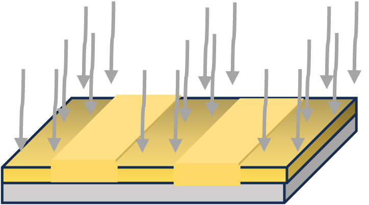 UV exposure (optional) | ZBA 21, 30kV e-beam E0 12 uC/cm2 | ZBA 21, 30kV e-beam E0 8 uC/cm2 |
| UV E0 30 mJ/cm2 | UV E0 24 mJ/cm2 | |
Cross-linking bake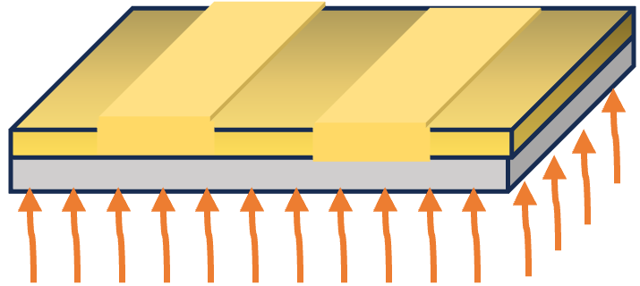 | 105 °C, 2 min hot plate or 100 °C, 60 min convection oven | |
| Development 21-23℃ puddle 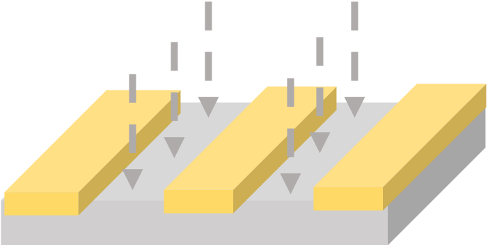 | AR 300-46, 60 sec | AR 300-46, 4:1, 60 sec |
Rinse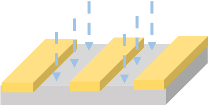 | DI water, 30 sec | |
| Post-bake (optional) 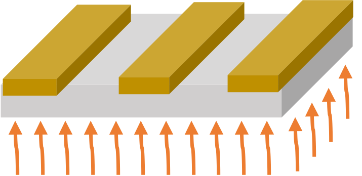 | 120 ℃ x 1 min hot plate, or 120 ℃ x 25 min convection oven for slightly enhanced plasma etching resistance | |
| Customer specific process 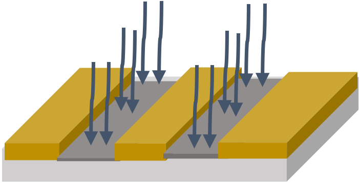 | Generation of semiconductor properties | |
Removal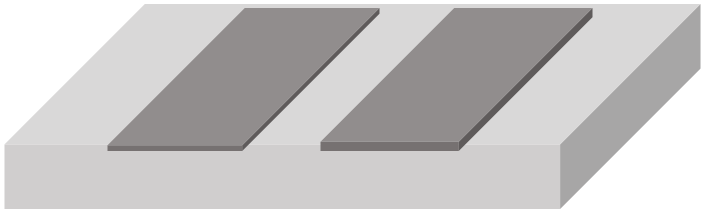 | AR 300-73, or O2 plasma ashing | |
…
Development recommendation
…
Process instruction 製程說明
These resists are predestined for e-beam exposure, but also suitable for UV exposure. During e-beam exposure, the resist works in a negative mode.
The exposure dose mainly depends on the acceleration voltage, the substrate and the film thickness. The resist also work in a negative mode after deep UV exposure if the image-wise exposure is performed at a wavelength of 248-265 and 290-330 nm.
A bake step is mandatory after exposure (e-beam/UV) to induce the required crosslinking.
Contrast and development rate strongly depend on the tempering. Recommended is a temperature of 105 °C (hot plate, 2 min), with possible variation of ± 5°C. Higher crosslinking temperatures require stronger developers. Contrast and development rate can be influenced to a large degree if developer strength and tempering temperature are coordinated accordingly. The general rule is the weaker the developer, the higher is the contrast and the lower the development rate. The development time ideally is about 60 s (30 … 120 s) at 21 – 23 °C. Shorter times for complete development will attack the crosslinked structures.
AR-N 7700系列是設計為電子束微影阻劑,但也適合於紫外線曝光. 在電子束曝光下為負型模式.
曝光劑量與加速電壓,基板種類及膜厚有關. 在深紫外線波長 248-265nm及390-330nm下曝光亦為負型模式.
曝後烤為促使阻劑產生架橋的必要程序. 阻劑的對比度與顯影速率與曝後烤有關. 建議的基本參數為105℃ ±5℃在熱板上烤2分鐘. 較高的架橋(曝後烤)溫度需使用較強的顯影劑. 顯影劑的選擇與架橋(曝後烤)溫度的搭配,直接影響對比與顯影速率. ㄧ般的原則是:較弱的顯影劑會有較高的對比與較低的顯影速率. 理想的顯影時間為在21 -23℃下顯影60 sec. (30 – 120 sec). 短時間就完全顯影容易有顯影劑攻擊已架橋的結構.
…
Proximity effect 鄰近效應
If electrons are used for the irradiation of resist films, always a certain amount of scattered radiation will occur, either as forward scattering due to an interaction with the resist material or as backscattering from the substrate (wafer). This phenomenon is called proximity effect and results in undesirable changes of the structures. The proximity effect is significantly more pronounced if sensitive resists (CAR) as compared to e.g., PMMA resists are used.
In the following example, AR-N 7700.18 was applied by spin coating to yield a film thickness of 1100 nm, tempered (85 °C, 2 min, hot plate) and irradiated with different doses (20 kV). The crosslinking bake was carried out at 105 °C, 3 min on a hot plate. After development (AR 300-46 undilute., 2 min), the following structures were obtained. Clearly visible is an increased widening of the 250-nm bars with higher exposure doses.
電子束曝光時,總有ㄧ部份電子會產生散射. 前向散射來自電子束與阻劑材料的相互作用; 反向散射則來自基板. 此現像稱為鄰近效應. 鄰近效應會導致所寫的圖案結構改變. 比起像PMMA阻劑,化學放大型阻劑的鄰近效應較明顯.
如下圖以AR-N 7700.18為例, 膜厚1100nm, 軟烤85℃ x 2 min(熱板), 以20kV加速電壓做不同劑量曝光. 隨後在熱板上以105℃ x 3min做曝後烤. 顯影(AR 300-46 x 2 min)後結構如下圖. 曝光劑量越高底部變寬現像越明顯.
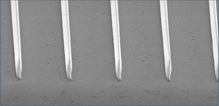
AR-N 7700.18 dose 19.5 μC/cm2

AR-N 7700.18 dose 37.0 μC/cm²
AR-N 7700.18 dose 63.5 μC/cm²
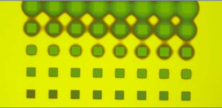
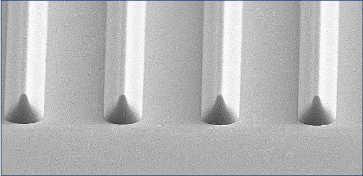
Dose sequence of AR-N 7700.08 : Squares were written with a dose of 1.0 – 90 μC/cm². The proximity effect at higher dosesis quite apparent.
…
