AR-N 7500 series standard negative e-beam lithography resist
High resolution process stable resist for mix and match process
…
Product brief 產品簡介
AR-N 7500系列, 為負型電子束微影阻劑 (negative tone EBL resist). 可在電子束及紫外光波長曝光(deep UV, I line, G line), 適合於半導體混搭製程(mix & match). 產品系列目前有:
AR-N 7500.08
AR-N 7500.18
…
Product series & Code 產品比較及編碼說明:

…
Packing 產品包裝:
✅ 250 ml /瓶
✅ 1 L /瓶
其它包裝可依客戶需求增加.
Shipping 出貨:
本品未列於固定生產品項,價格交期需先詢問,
預估交期為
✅ 4 – 8 週. 徳國運出
…
Product Features 產品特性
- e-beam, deep UV, i-line, g-line
曝光波長為電子束,深紫外線,i-line,g-line - intermediate sensitivity
中等敏感度 - mix & match-processes between e-beam and UV exposure 310 – 450 nm, positive or negative depending on the exposure wavelength chosen
適合電子束與紫外線 (310-450 nm)的混搭製程. 依曝光波長決定其為正型或負型特性. - high resolution, process-stable (no CAR)
非化學放大型,但解析度高,製程穩定
- plasma etching resistant, thermostable up to 120 °C
耐乾蝕刻, 高溫穩定性達120℃ - novolac, naphthoquin. diazide, organic cross-linking agent
主要成份含酚醛樹酯, 疊氮基萘醌, 有機物架橋劑等 - safer solvent PGMEA
溶劑使用較安全的丙二醇甲醚醋酸酯
…
Product Properties 產品物性
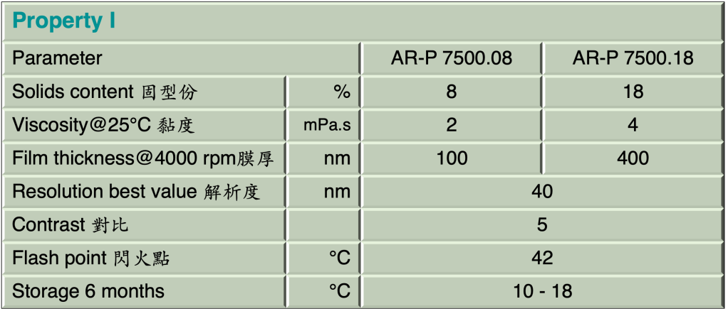
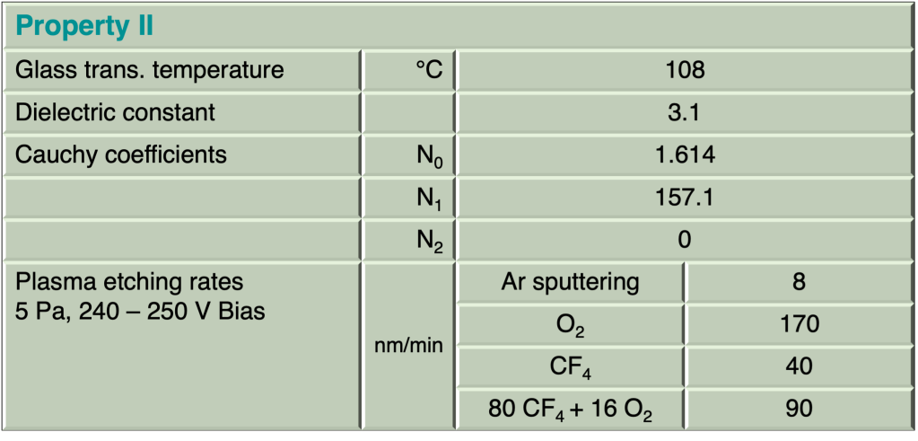
…
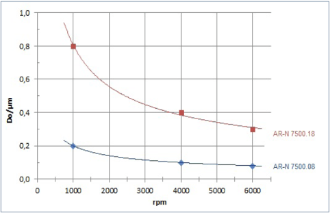
Spin curve 塗佈曲線
…
Structure resolution
AR-N 7500.18 Film thickness 400 nm
Lattice with 70 nm lines
Resist structures
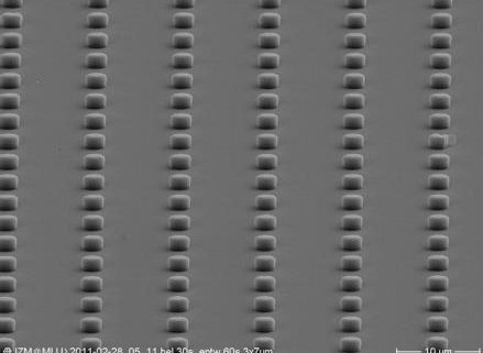
AR-N 7500.18, rows of cylinders with a diameter of 500 nm
Process parameters
| Substrate | 4″ Si wafer |
| Soft bake | 85℃ 90sec, hot plate |
| Exposure | ZBA 21, 30kV |
| Development | AR 300-47 4:1, 60sec 22℃ |
…
Process baseline 製程參數
This diagram shows exemplary process steps for AR-N 7500 resists. All specifications are guideline values which
have to be adapted to own specific conditions. For further information on processing, 👉 “Detailed instructions
for optimum processing of e-beam resists”. For recommendations on waste water treatment and general safety
instructions, 👉”General product information on Allresist e-beam resists”.
表列為AR-N 7500阻劑產品製程參數的範例. 所有參數為參考值,使用者應依設備環境實際狀況加以調整
| AR-N 7500.18 | |
Coating | 400 nm@4000 rpm x 60 sec |
Soft bake (± 1℃) | 85℃ x 2 min hot plate, or 85℃ x 30 min, convection oven |
e-Bean exposure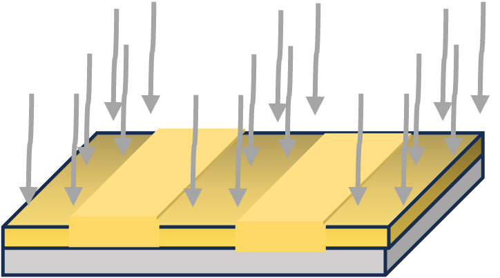 | ZBA 21, 20kV Exposure dose (E0): 180 μC/cm2 |
Development (21-23±0.5℃) puddle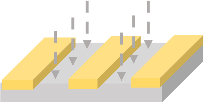 | AR 300-47, 4 : 1, 60 sec |
Rinse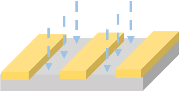 | DI water, 30 sec |
Post-bake (optional) | 120 °C, 1 min hot plate or 120 °C, 25 min convection oven for enhanced plasma etching resistance |
Customer specific technology | Generation of semiconductor properties |
Resist removal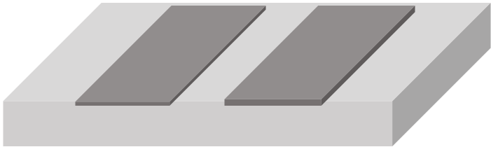 | AR 300-76, or O2 plasma ashing |
…
Development recommendation
…
Exposure for negative & positive
These resists are predestined for e-beam exposure, but also suitable for UV exposure. Mix & match processes are possible, if both exposure methods are carefully coordinated. During e-beam exposure, the resist works in a negative mode. If these resists are exposed to UV, they also work in a negative mode if image-wise exposure is performed at 310 to 365 nm, followed by flood exposure at > 365 nm (optimum g-line). The exposure dose is in this case roughly 100 mJ/cm2 (i-line) for a film thickness of 400 nm. With an additional tempering step (85 °C, 2 min hot plate) after image-wise exposure, the sensitivity can be slightly increased. A positive image is obtained after image-wise UV exposure at 365 – 450 nm without subsequent flood exposure. The developer dilution should be adjusted with DI water in such a way that the development time is in a range of 30 and 120 s at 21 – 23 °C.
AR-N 7500系列是設計為電子束微影阻劑,但也可在紫外線曝光. 兩種曝光參數經適當調配,可用於半導體混搭製程(mix & match).
阻劑在電子束曝光下為負型模式. 在紫外線波長310 – 365下曝光,其作用亦為負型模式, 通常需以g-line加曝(波長>365nm).
膜厚400nm在紫外光i-line下曝光,約需100mJ/cm2的劑量. 曝光後在熱板以85℃ x 2 min進行曝後烤可提高敏感度.
如果在紫外線365 – 450nm下曝光且不做加曝流程,則阻劑呈現正型模式.
顯影劑濃度視需要以純水調整,建議的顯影時間,溫度為20 – 120 sec, 21 – 23℃.
…
