Conductive Coating AR-PC 5090.02 (Electra 92)
Top layer dissipation of electron beam charges on insulating substrate
Conductive protective coating for non-Novolac-based e-beam resists
…
Electra 92 Product Brief 產品說明
Electra 92 應用於電子束微影或顯微鏡分析,於絕緣基板上塗佈導電層,使電子束曝光時電荷得以逸散.目前有三種產品系列,編號為:
AR-PC 5090.02 適用於:非酚醛樹酯,PMMA,共聚高分子(例:CSAR 62)及HSQ (例Medusa 82)。
AR-PC 5091.02 適用於酚醛樹酯類為基礎的電子束微影阻劑。
AR-PC 5092.02 無選擇性,適合目前各類型阻劑。溶於水,於SEM後,試片不會破壞,仍可使用。
…
Electra 92 product comparison 產品比較
| Properties | AR-PC 5090.02 | AR-PC 5091.02 | AR-PC 5092.02 | |
| Solid content (固型份) | % | 2 | 2 | 2 |
| Viscosity (黏度) | mPas | 1 | 1 | 1 |
| Thickness (厚度) vs Spin speed (轉速) | nm rpm | 42 – 100 @ 4000 – 1000 | 31 – 80 @ 4000 – 1000 | 42 – 100 @ 4000 – 1000 |
| Specific conductivity (@60nm FT)導電度 | S/m | ~100 | ~100 | ~100 |
| Conductive polymer (高分子類型) | polyaniline-derivative | polyaniline-derivative | polyaniline-derivative | |
| Solvent (使用溶劑) | Water & IPA | Water & IPA | Water | |
| Resist compatibilities (適用阻劑類型) | non-novolac PMMA co-polymer (CSAR 62) HSQ (Medusa 82) | novolac base resist | (universal type) novolac base resist PMMA co-polymer (CSAR 62) HSQ (Medusa 82) and others | |
…
AR-PC 5090.02 packing & shipping
Packing 產品包裝:
✅ 100 ml/瓶
✅ 250 ml/瓶
✅ 1 L/瓶
其它包裝可依客戶需求增加.
Shipping 出貨:
✅ 2 – 4 週: 徳國運出
❎ 1 週: 國內庫存
(目前暫無國內庫存)
…
AR-PC 5090.02 Features 產品特性
- as protective coating, this resist is not sensitive to light / radiation
此導電保護塗佈材料對光/輻射不感應. - thin, conductive layers for the dissipation of charges during electron exposure
塗佈形成導電薄膜使電子束曝光時,電荷得以逸散 - coating of non-novolac PMMA, CSAR 62, HSQ et al
適用於非酚醛係EBL阻劑,例如: PMMA, CSAR 62, HSQ等 - long term stable
長期穩定性良好 - easy removal with water after exposure
曝光後可輕易以水去除 - polyaniline-derivative dissolved in water and IPA
主要成分為溶於水及IP A的聚苯胺衍生物
…
Product properties 產品物性
| AR-PC 5090.02 Property I | ||
| Parameter | AR-PC 5090.02 | |
| Solid content 固型份 | % | 2 |
| Viscosity@25℃ 黏度 | mPas | 1 |
| Film thickness@4000 rpm 膜厚 | nm | 42 |
| Film thickness@1000 rpm膜厚 | nm | 100 |
| Resolution / Contrast | nm/– | – – |
| Flash point 閃火點 | ||
| Storage temperature* 儲存溫度 | ℃ | 8 – 12 |
| * Product is guaranteed 6 months shelf life from the data of sale if stored correctly. 在正確的儲存條件下,產品保證的有效期為銷售日起6個月. * Product can also be used without guarantee until the date indicated on the label. 在無提供保證的情況下,產品可使用至標籤上所示的有效期. | ||
| AR-PC 5090.02 Property II | ||
| Conductivity (@ 60nm FT) | S/m | 1.2 |
| Cauchy coefficients | N0 | — |
| N1 | — | |
| N2 | — | |
| Plasma etching rate (nm/min) 5 Pa. 240-250 V Bias) | Ar-sputtering | — |
| O2 | 185 | |
| CF4 | 68 | |
| 80 CF4 + 16 O2 | 120 | |
…
Conductivity 導電度
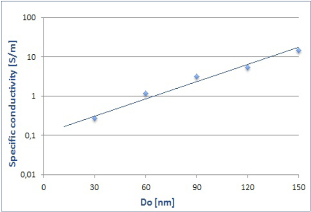
Conductivity measurements of AR-PC 5090.02 layers obtained after spin
deposition. For thinner films, the resistance increases and the conductivity decreases.
AR-PC 5090.02的導電度於塗佈後測得. 膜厚越低,其導電阻抗增加而導電度下降. 如圖.
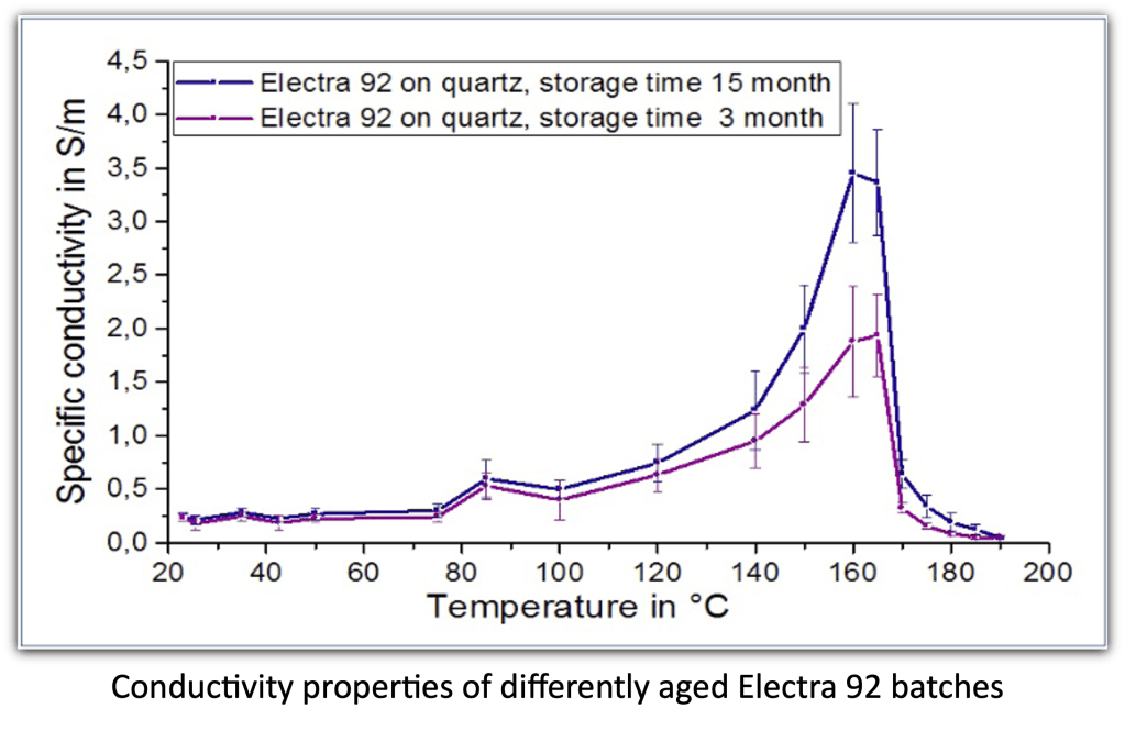
Conductivity Electra 92 as a function of Temperature
The conductivity was determined as a function of the measured temperature. At temperatures < 100 °C, both resists show a virtually identical conductivity. Conductivity measurements up to a temperature of 160 °C which were performed directly on a hotplate showed a large increase of the conductivity by a factor of 10 (see diagram). This fact is due to the complete removal of water from the layer. After a few hours of air humidity absorption under room conditions, the conductivity decreases again to the initial value. In the high vacuum of e-beam devices, the water is also completely removed and the conductivity thus increases accordingly. This effect has been demonstrated in direct conductivity measurements under mediate vacuum conditions. Temperatures above 165 °C destroy the polyaniline irreversibly and no conductivity is observed any more.
- 導電度會受環境溫度影響 (如圖,兩種不同置放時間的試片):
- 當溫度低於100℃時,兩者導電度幾乎沒有差異.
- 試片於熱板上加熱至160℃時,由於水份移除,導電度增加達10倍.
- 於室溫中置放幾個小時後,由於吸濕,導電度恢復原來數值.
- 在高度真空的電子束微影設備中,水份幾乎不存在,因此導電度會比室溫量測值高. 在中度真空條件下量測導電度已驗證此項效應.
- 溫度超過165℃會破壞聚苯胺高分子,因此不再有導電度.
…
REM dissipation of charge 電荷逸散實例
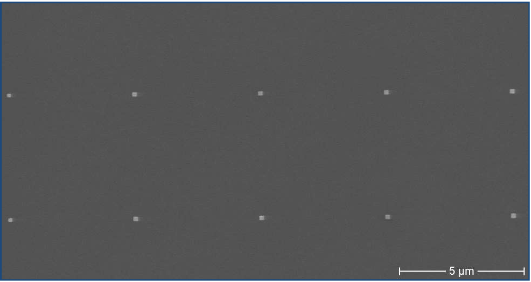
200 nm-squares written on quartz without distortion caused by charges with AR-P 662.04 and Electra 92
在石英基板上以電子束微影寫出不變形的200 nm-squares圖案.
石英基板上的材料是AR-P 662.04 PMMA resist及Electra 92導電塗佈.
| Process parameters | |
| Substrate | 4“ wafer quartz with AR-P 662.04 |
| Coating | 60 nm @ 2000 rpm |
| Soft bake | 85℃ |
| — | |
| Process chemicals | |
| Adhesion promoter | — |
| Developer | — |
| Thinner | — |
| Remover | DI-water |
…
Process baseline 製程參數
| Conductive coating of PMMA resist Thsi diagram shows exemplary process steps Electra92 (AR-PC 5090.02) and PMMA resist AR-P 664.04. All specifications are guideline values which have to be adapted to own specific conditions. | |||
| 1st Coating |  | AR-P 662.04 on insulating substrate (quartz, glass, GaAs) 140nm@4000rpm x 60sec | |
| 1st soft bake (±1℃) |  | 150 ℃ x 2 min hot plate, or 150 ℃ x 30 min convection oven | |
| 2nd Coating | 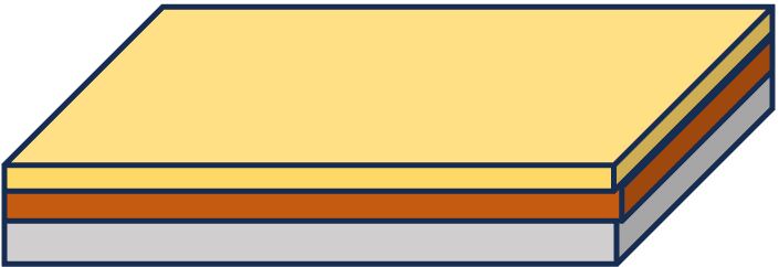 | AR-PC 5090.02 60nm@2000rpm x 60sec | |
| 2nd tempering (±1℃) |  | 90°C x 2min hot plate or 85°C x 25min convection oven | |
| e-Beam exposure | 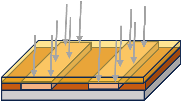 | ZBA 21, 20 kV Exposure dose (E0): 110 uC/cm2 (AR-P 662.04, 140nm) | |
| Removal Conductive layer |  | AR-PC 5090.02 DI water, 60sec | |
| Development puddle (21-23 ± 0.5℃) |  | Resist: AR-P 662.04 Developer: AR 600-56 x 2min Stopper: AR 600-60 x 30sec | |
| Post-bake (optional) |  | 130°C x 1min hot plate or 130°C x 25min convection oven for slightly enhanced plasma etching stability | |
| User specific process | 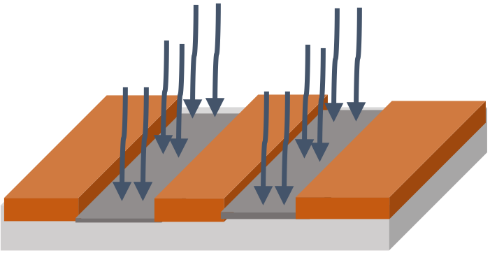 | Generation of e.g. semiconductor properties, etching, sputtering…. | |
| Removal |  | AR 600-71 or O2 plasma ashing | |
| Process hints The conductivity may be varied by adjusting the thickness with different rotational speeds. Thicker layers of 90 nm thus have a 2.5 times higher conductivity as compared to 60 nm thick layers. In the case that crack formation is observed after tempering of the protective coating, the tempering step can be omitted. For the build-up of an even conductive layer, the substrate should be wetted with the resist solution before the spin process is started. After a certain storage time at room temperature, the coating pattern of Electra may change slightly. To restore the coating pattern, treatment with ultrasound and filtration (0.2 um) can then be carried out. 導電度可依導電層厚度加以調節. 90nm厚的導電層比60nm厚其導電度高約2.5倍. 導電層如果於軟烤厚產生裂痕,可跳過軟烤製程,以避免裂痕產生. 導電層塗佈前先以阻劑的溶劑濕潤基板可獲得較均勻的厚度. 導電材料Electra 92如果置於室溫下太久,會使塗佈參數稍為改變. 處以超音波及0.2um過濾可使其恢復. | |||
…
Application example
…
CSAR on glass
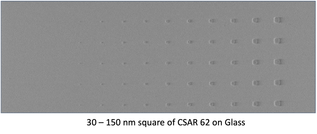
The combination of CSAR 62 with Electra 92 offers the best options to realise complex e-beam structuring processes on glass or semi-insulating substrates like e.g. gallium arsenide. The excellent sensitivity and highest resolution of the CSAR are complemented harmoniously by the conductivity of Electra 92.
電子束微影阻劑搭配AR-PC 5092.02導電塗佈, 提供奈米微影製程更佳的選擇性. 例如在玻璃基板,或是GaAs等半絕緣的基板上完成電子束微影的複雜結構.
高敏感度與高解析度的EBL阻劑CSAR 62與導電塗佈Electra 92是電子束微影中完美的搭配.
| At a CSAR 62 film thickness of 200 nm, squares with an edge length of 30 nm could reliably be resolved on glass. | |
| Substrate | Glass 24 x 24 mm |
| Adhesion AR 300-80 | 4000 rpm; 10 min, 180 °C hot plate |
| Coating AR-P 6200.09 | 4000 rpm; 8 min, 150 °C hot plate |
| Coating AR-PC 5092.02 | 4000 rpm; 5 min, 105 °C hot plate |
| E-Beam irradiation | Raith Pioneer, 30kV, 75uC/cm2 |
| Removal Electra 92 | 2 x 30 sec water, dipping bath |
| Bath (drying) | 30 sec AR 600-60 |
| Development CSAR 62 | 60 sec AR 600-546 |
| Stopping | 30 sec AR 600-60 |
…
PMMA lift-off on glass
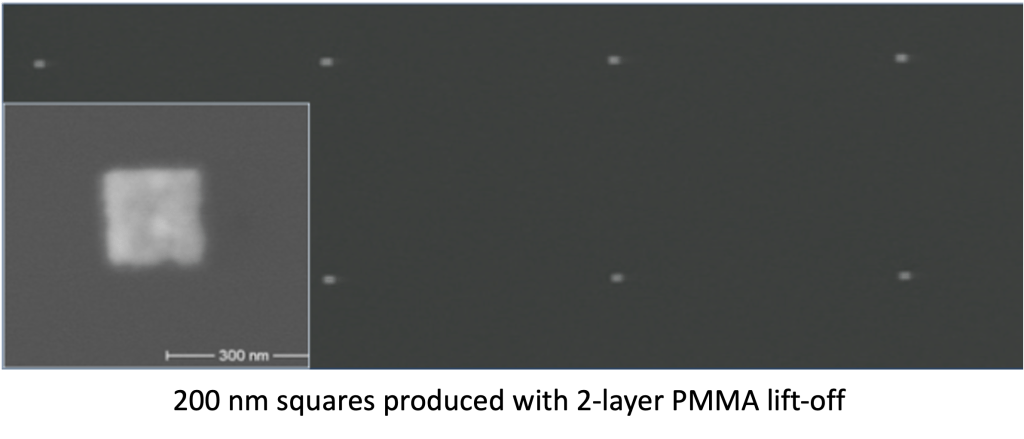
Initially, the PMMA resist AR-P 669.04 (200 nm thickness) was coated on a quartz substrate and tempered. The second PMMA resist AR-P 679.03 was then applied (150 nm thickness) and tempered, followed by coating with Electra 92. After exposure, Electra 92 was removed with water, the PMMA structures were developed (AR 600-56) and the substrate vaporized with titanium/gold. After a liftoff with acetone, the desired squares remained on the glass with high precision.
在石英基板上做 PMMA lift-off 製程, 程序如下:
- 塗佈PMMA AR-P 669.04 (200nm厚) 並軟烤
- 塗佈PMMA AR-P 679.03 (150nm厚) 並軟烤
- Electra 92導電塗佈
- 電子束曝光,並將Electra 92以DI water去除
- 以AR 600-56顯影, 完成PMMA結構並進行鈦Ti/金Au 蒸鍍
- 以丙酮進行lift-off結構去除, 在石英基板上留下設計的精密結構
| Parameters | |
| Substrate | Glass 25 x 25 mm |
| Coating AR-P 669.04 | 4000 rpm; 3 min, 150 °C hot plate |
| Coating AR-P 679.03 | 4000 rpm; 3 min, 150 °C hot plate |
| Coating AR-PC 5092.02 | 2500 rpm; 5 min, 105 °C hot plate |
| E-beam irradiation | Raith Pioneer; 30 kV, 75 μC/cm2 |
| Removal Electra 92 | 2 x 30 sec water |
| Development PMMAs | 60 sec AR 600-56 |
| Stopping | 30 sec AR 600-60 |
| metal deposition & lift off | titanium/gold |
…
HSQ on quartz
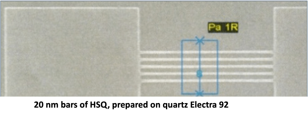
After a coating of Electra 92 on an HSQ resist, even this resist can be patterned on a quartz substrate with very high quality. The HSQ resist (20 nm thickness) was irradiated with the required area dose of 4300 μC/cm². Electra 92 was subsequently completely removed within 2 minutes with warm water and no residues could be detected. After development of the HSQ resist, the structures with high-precision 20 nm bars remained.
塗佈Electra 92於已有HSQ阻劑的石英基板電子束微影劑量4300 uC/cm2 (HSQ厚度約20nm)以溫水浸泡約2 min可完全去除Eectra 92導電層 顯影HSQ阻劑,可得20nm寬的高精密條狀結構
…
Lift-off structure on garnet
…
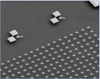
Plasmonic structure on quartz
…
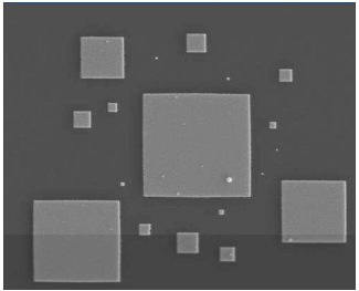
On highly insulating substrate for SEM application
Electrostatic surface charges caused by a deflection of the incident electron beam can be extremely disturbing and interfere with a correct imaging. To avoid this effect, e.g. gold is evaporated onto the sample which however also entails disadvantages since some structures change irreversibly due to thermal effects. Studies demonstrated that the conductive coating Electra 92 can be used as alternative. The coating on electrically highly insulating polymers or glass also enables high-quality images of nanostructures in SEM:
電子顯微鏡應用時,電子束反射所產生的靜電表面電荷會干擾成像. 解決方法可在樣品上蒸度金層, 但蒸鍍時產生的溫度易使樣品變型.研究以Electra 92導電塗層取代蒸鍍,在高絕緣材料,如聚合物,玻璃等,可獲得高品質的奈米結構影像.
After SEM investigation, the conductive coating was completely removed with water, and structures could still be used further.
SEM檢查後,導電層以水洗除,樣品可持續使用
…
