Laser ablation of PPA (Phoenix 81)
PPA layers can also be structured by laser ablation. Substrates coated with AR-P 8100 were structured with pulsed laser light at different wavelengths at the IOM Leipzig (Dr. Klaus Zimmer). In this process, architectures with very little edge roughness could be generated. In the absorption range of PPA, at 248nm, complete ablation was achieved without damaging the silicon substrate.
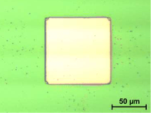

Fig. 1 and 2: 0,5 J/cm2, 248nm, 20ns, double-pulse exposure, 700nm PPA on Si-wafer
Although PPA shows only very little absorption at a wavelength of 355nm, selective ablation with comparatively high sensitivity is still possible. The generated structures again show very smooth edges.

Fig. 3: 0,1 J/cm2, 355nm ps-laser, single-pulse exposure, 700nm PPA on Si-wafer
The laser beam can also be used for the generation of 3d structures. Interference projection through a phase mask allows the generation of grid structures with sinusoidal course and very little surface roughness.
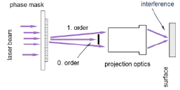
Fig 4: experimental structure interference projection


Fig. 5 and 6: SEM micrograph of generated PPA grid with sinusoidal course (period ~750nm); 248nm, 20ns pulse, number of pulse: 10, 700nm PPA on Si-wafer
Overview of photoresist-others
Alkali-stable positive resist obtained after treatment with HMDS
Aqueous negative resist based on gelatine
Atlas 46 for nanoimprint lithography
Ethanol and toluene-resistant photoresist AR-U 4060
Fluorescent resist structures with photoresists
Laser ablation of PPA (Phoenix 81)
Negative CAR PMMA resist SX AR-N 4810/1
Positive polyimide one-layer resist
Resist for near infrared (NIR)
Structuring by ablation of the resist materials
Structuring of polyphthalaldehydes with photolithography
Surface imaging resist system SX AR-N 7100 – silylable photoresist
Top surface imaging (TSI) photoresist – principles
Two-layer photoresist system for water-sensitive substrates
Two-layer resist system for hydrofluoric acid etching
