Black resist
For a surprisingly high number of applications, it is important to disable the transparency of the substrates completely, while still having the option to generate structures. The optically protected area should possibly cover the whole UV/VIS range from 200 – 1.000 nm. For the area of 200 -350 nm this is quite simple, since the resist components already absorb sufficiently there. For wave lengths > 350 nm, colorants must be added, which generate the desired absorption for longer waves.
We now have developed a resist which fulfills the requirements. First experiments resulted in a sufficiently high absorption up to 800 nm, the layer thus can be regarded as optically dense. We have mixed a negative resist with black and dark blue colorants and measured the absorption of the resulting layer thickness. Fig. 1 shows the absorption spectrums. At a thickness of 23 µm, the area of 300 – 800 nm is optically dense.
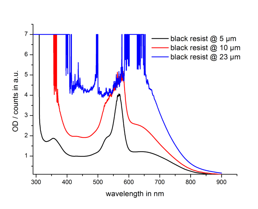
Fig. 1 UV/VIS spectrums of the black resist layers
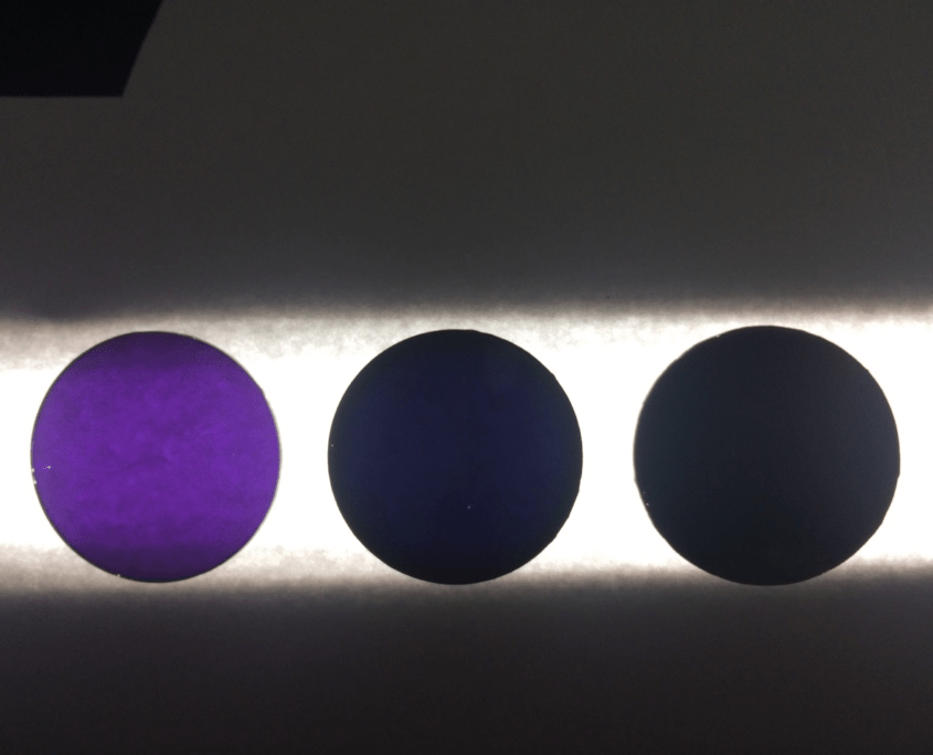
Fig. 2 Visual image of the optical density (5 µm, 10 µm, 23 µm)
Even at a layer thickness of 23 µm, structuring is still possible. Common photolithography can be used here. This layer, however, needs a very strong aqueous-alkaline developer (AR 300-26 or AR 300-73 1 : 1 diluted).
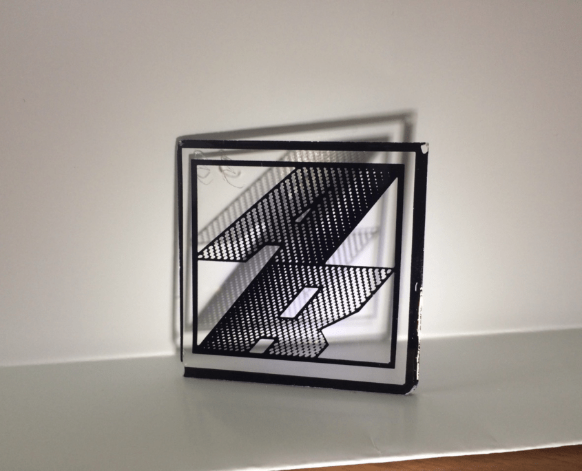
Fig. 3 AR logo structures in black resist
Overview of photoresist-others
Alkali-stable positive resist obtained after treatment with HMDS
Aqueous negative resist based on gelatine
Atlas 46 for nanoimprint lithography
Black resist
Ethanol and toluene-resistant photoresist AR-U 4060
Fluorescent resist structures with photoresists
Laser ablation of PPA (Phoenix 81)
Negative CAR PMMA resist SX AR-N 4810/1
Positive polyimide one-layer resist
Resist for near infrared (NIR)
Structuring by ablation of the resist materials
Structuring of polyphthalaldehydes with photolithography
Surface imaging resist system SX AR-N 7100 – silylable photoresist
Top surface imaging (TSI) photoresist – principles
Two-layer photoresist system for water-sensitive substrates
Two-layer resist system for hydrofluoric acid etching
