Forays through the lithography of microelectronics
Author: Matthias Schirmer
Introductory Remarks
Due to the fast-paced development of photolithography since the 1990s, only a short summary of the different techniques and applications can be given here. For in-depth information on the multitude of facts, technologies and procedures presented in each chapter, the added references should be consulted.
As of: 2020-01-27
1. Brief History of Imaging Techniques
Imaging for microelectronics is rooted in both printing technology and photography. Already in the 1st century AD, the Diamond Sutra (“The diamond that cuts through illusion”) was produced in China with wood block printing. Each character was carved mirror-inverted into a wooden panel, the shapes then rubbed in with colour and pressed onto paper. By these means, a text could also be reproduced. A revolutionary improvement was Gutenberg’s letterpress in 1450. Movable metallic letters placed in a printing frame allowed for the first time to produce many copies of a text.
The first imaging technique involving light was developed about 1826 by Joseph Nicephore Niépce who invented the first real photolithography method [1, 2]. The Greek words photo (-> light), litho (-> stone) and graphic (-> writing) exactly describe this process. Niépce used a special form of bitumen which he coated onto a tin plate and exposed with a “camera obscura” for eight hours. Bitumen hardens under the influence of light, and the non-hardened areas were subsequently washed out with lavender oil.
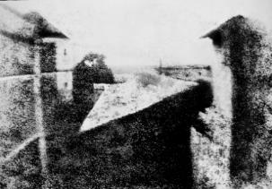
Fig.1 First photograph by Niépce 1826 (retouched reproduction, 1952)1)
to be continued
Overview of basic chemistry
forays through the lithography of microelectronics
