T-gates with three-layer system
Publication MNE 2017
T-gate structures are often required for the fabrication of electronic components (MEMS, HEMTs). Corresponding nanostructures can be realized via e-beam lithography in multi-layer processes. Generally, resist layers with different sensitivities like e.g. PMMAs with varying molecular weight distributions are coated on top of each other, irradiated with electrons and then developed in one step. For the production of more defined architectures it is however advantageous to combine different types of resists. In this case, not only the mixing of the different layers during coating can be avoided, but also the use of selective developers is possible. As a result, high contrasts and accurate undercuts can be achieved.
The following resist combination was evaluated at the Martin Luther University in Halle (AG Prof. G. Schmidt) with great success:
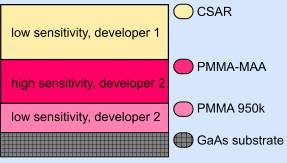
Fig. 1 Resist architecture for the fabrication of T-Gates
CSAR 62 was used as top layer; the development was carried out with AR 600-546 (amyl acetate). In this high-contrast developer, CSAR 62 and also the lower layer consisting of 950k PMMA (AR-P 679.03) has a relatively low sensitivity. In the intensively irradiated (30 kV) central area, nevertheless a complete development of all layers is achieved.
Subsequently, the undercut in the middle layer (PMMAcoMA 33, AR-P 617) can be produced in a second development step with X AR 600-50/2.
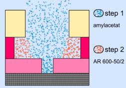
Fig. 2 Schematic sketch of development steps 1 and 2
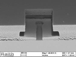
Fig. 3 3D-resist profile after development and prior to the metallization step
The special developer X AR 600-50/2 selectively develops the middle layer. The three-layer process as described above enables the fabrication of three-dimensional nanostructures with high contrast in only one electron exposure. The process window is wide, and the shape of the undercut as well as the geometry of the lower PMMA layer can be easily modified. After metallization and lift-off, T-gate architectures as well as nanoscale metal bridges could be realized.

Fig. 4: T-gate after lift-off

Fig. 5: Metal bridge structures
Related articles EBL positive
CSAR 62 related
3-layer system CSAR/PMMAcoMA/PMMA
3-layer system for T-gate CSAR/PMMAcoMA/PMMA
BOE etching of SiO2 with CSAR 62 mask
Collapse of extreme high-resolution e-beam resist structures
CSAR 62 Avoidance of particles during large-area exposures
CSAR 62 – Development at low temperatures
CSAR 62 – Experimental studies on new, sensitive developers
CSAR 62 lift-off for thick layers
CSAR 62 nanostructures written at 100 kV
CSAR 62 single layer lift-off system
Evaluation of various developers for e-beam exposed CSAR 62 layers (100 kV)
HF etching of GaAs with CSAR 62 masks
Manufacture of plasmonic nanostructures with CSAR 62
Use of CSAR 62 for the manufacture of nanostructures on GaAs substrates
