PMMA e-beam resist with flat gradation for three-dimensional structures
It is advantageous for the fabrication of three-dimensional structures if the gradation (contrast) is low (see also Resist Wiki 3.2.3, Diffractive optics with “analogue” e-beam resist). A resist with very high contrast will always generate perpendicular resist flanks. Smallest changes of the dose induce a rapid shift from undeveloped to the completely developed state. If the gradation is low, the dose difference between the undeveloped and the completely developed state is accordingly high. If parallel lines are written with increasing dose, a stepped structure is obtained which is much more pronounced as compared to the high contrast.

Abb. 1 Negative-e-beam resist step wedge after exposure with a dose range
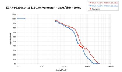
Allresist has designed a PMMA resist which is characterised by a very flat gradation. A crosslinking agent was added to the PMMA resist. During irradiation, two competing processes occur: the positive process, in which the polymer chain is split; producing small fragments which are readily soluble in the developer, and the negative process, in which the polymer chains and also the fragments are crosslinked again. Optimising the content of the crosslinking agent is of great importance for a flat gradation. Fig. 1 shows two contrast curves of the experimental samples SX AR-P 6210/14-15 which cover a dose range between approximately 80 μC/cm2 and 2000 μC/cm2. The gradation is less than 1.
PMMA resists of the SX AR-P 6210 series are particularly well suited for the fabrication of three-dimensional structures.
Related articles EBL positive
CSAR 62 related
3-layer system CSAR/PMMAcoMA/PMMA
3-layer system for T-gate CSAR/PMMAcoMA/PMMA
BOE etching of SiO2 with CSAR 62 mask
Collapse of extreme high-resolution e-beam resist structures
CSAR 62 Avoidance of particles during large-area exposures
CSAR 62 – Development at low temperatures
CSAR 62 – Experimental studies on new, sensitive developers
CSAR 62 lift-off for thick layers
CSAR 62 nanostructures written at 100 kV
CSAR 62 single layer lift-off system
Evaluation of various developers for e-beam exposed CSAR 62 layers (100 kV)
HF etching of GaAs with CSAR 62 masks
Manufacture of plasmonic nanostructures with CSAR 62
Use of CSAR 62 for the manufacture of nanostructures on GaAs substrates
