HF etching of GaAs with CSAR 62 masks
Mr. Y. Nori from Lancaster University (Department of Physics, UK) could very successful generate structures for the production of photonic crystals with CSAR 62. These structures serve as a starting point for the production of GaSb „quantum dots“ which can be applied as single photon emitters. For this purpose, at first a layer of Al0.8GaAs0.2 was established on a GaAs substrate, followed by deposition of a GaAs layer in which GaSb „quantum dots“ were embedded. For the preparation of the photonic crystal, CSAR 62 was applied onto the modified substrate and patterned by e-beam lithography. Subsequently, developed structures were transferred by plasma etching into the upper GaAs layer and finally under-etched by wet chemical etching with HF to produce bridging architectures.
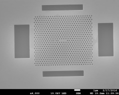
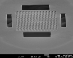
Fig. Structures in GaAs 62 produced with CSAR 62 and ICP etching; bridging GaAs structures after HF etching
Critical for a successful realisation of GaAs-bridges was the higher plasma etching stability of CSAR 62 as compared to PMMA. It furthermore became evident that at 100°C, a much more favourable etching ratio of GaAs to CSAR 62 can be observed: the etching ratio of CSAR 62: GaAs was 1:3.64 at 100°C, but only about 1:1.9 at room temperature.
Related articles EBL positive
CSAR 62 related
3-layer system CSAR/PMMAcoMA/PMMA
3-layer system for T-gate CSAR/PMMAcoMA/PMMA
BOE etching of SiO2 with CSAR 62 mask
Collapse of extreme high-resolution e-beam resist structures
CSAR 62 Avoidance of particles during large-area exposures
CSAR 62 – Development at low temperatures
CSAR 62 – Experimental studies on new, sensitive developers
CSAR 62 lift-off for thick layers
CSAR 62 nanostructures written at 100 kV
CSAR 62 single layer lift-off system
Evaluation of various developers for e-beam exposed CSAR 62 layers (100 kV)
HF etching of GaAs with CSAR 62 masks
Manufacture of plasmonic nanostructures with CSAR 62
Use of CSAR 62 for the manufacture of nanostructures on GaAs substrates
