Thick CSAR 62
A few applications like e.g. the manufacture of deep etched structures by plasma etching require a processing of thick resist layers. Of major importance in this case is a high sensitivity, especially in electron beam lithography. With the highly sensitive resist CSAR 62, film thicknesses up to 800 nm (AR-P 6200.13) or even up to 1.5 μm (experimental sample SX AR-P6200/10) can be produced. Even thicker films of more than 2 micrometer can be generated by multiple coatings.
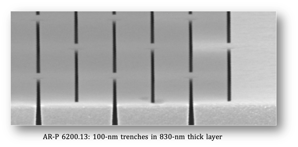
Fig. 1 AR-P 6200.13: 100 nm-trenches, height of the film 830 nm
Suitable as developer is AR 600-546. By varying the applied dose, the undercut can be specifically adjusted and provides structures from almost vertical edges up to pronounced lift-off architectures.
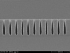
Dose: 1200pC/cm
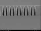
Dose: 1440 pC/cm
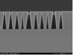
Dose: 1728 pC/cm
Fabrication of trenches at the MLU (single pixel lines, 30 keV, film thickness 830 nm, period 300 nm, dosage series, developer AR 600-546, 60 s, stopper IPA)
Related articles EBL positive
CSAR 62 related
3-layer system CSAR/PMMAcoMA/PMMA
3-layer system for T-gate CSAR/PMMAcoMA/PMMA
BOE etching of SiO2 with CSAR 62 mask
Collapse of extreme high-resolution e-beam resist structures
CSAR 62 Avoidance of particles during large-area exposures
CSAR 62 – Development at low temperatures
CSAR 62 – Experimental studies on new, sensitive developers
CSAR 62 lift-off for thick layers
CSAR 62 nanostructures written at 100 kV
CSAR 62 single layer lift-off system
Evaluation of various developers for e-beam exposed CSAR 62 layers (100 kV)
HF etching of GaAs with CSAR 62 masks
Manufacture of plasmonic nanostructures with CSAR 62
Use of CSAR 62 for the manufacture of nanostructures on GaAs substrates
