CSAR 62 single layer lift-off system
With our new development e-beam resist AR-P 6200 (CSAR 62), very fine structures like e.g. 10 nm wide trenches can be manufactured with very high contrast (> 14) and comparably high sensitivity.

Fig. 1: Max. resolution of CSAR 62 of 10 nm (180 nm).
or the writing of 10 nm wide trenches at a layer thickness of 180 nm, only an exposure dose (dose to clear) of 220 pC/cm was required (30 keV, developer AR 600-546). Due to the proximity effect, narrow trenches in the same size range with defined undercut can be created if a 1.5 – 2 times higher exposure dose is used
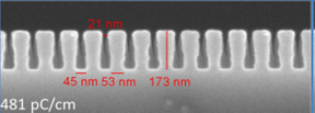
Fig. 2: Undercut structures due to increased exposure dose
Addition 03/2018
Results Prof. Smith, Massachusetts Institute of Technology, Cambridge USA
CSAR 62 (AR-P 6200.09) was coated at 4000rpm and exposed with 30kV by a Raith SEBL system. Lines with variable distance were generated in the range of von 400 nm up to bis zu 1000 nm. In order to avoid electrostatic charge, Electra 92 was used as top layer. Layer thickness 190nm, developer AR 600-546, development time 60s, stopper IPA. The developed resist architectures were evaluated in the REM.
Related articles EBL positive
CSAR 62 related
3-layer system CSAR/PMMAcoMA/PMMA
3-layer system for T-gate CSAR/PMMAcoMA/PMMA
BOE etching of SiO2 with CSAR 62 mask
Collapse of extreme high-resolution e-beam resist structures
CSAR 62 Avoidance of particles during large-area exposures
CSAR 62 – Development at low temperatures
CSAR 62 – Experimental studies on new, sensitive developers
CSAR 62 lift-off for thick layers
CSAR 62 nanostructures written at 100 kV
CSAR 62 single layer lift-off system
Evaluation of various developers for e-beam exposed CSAR 62 layers (100 kV)
HF etching of GaAs with CSAR 62 masks
Manufacture of plasmonic nanostructures with CSAR 62
Use of CSAR 62 for the manufacture of nanostructures on GaAs substrates
