CSAR 62 nanostructures written at 100 kV
Applying an acceleration voltage of 100 kV has the advantage that the proximity effect due to electron backscattering can be avoided. The suitability of CSAR 62 for the manufacture of complicated architectures was investigated in detail at the Karlsruhe Institute of Technology (KIT Institute of Microstructure Technology, Dr. Lothar Hahn). For this purpose, CSAR 62 layers were exposed at 100 kV using an EBPG5200Z e-beam writer and developed with our developer for high contrast, AR 600-546. The best results were obtained at an exposure dose of 225 μC/cm2 and a development time of 3 minutes. The developed structures were sputtered with Au/Pd and investigated by SEM.
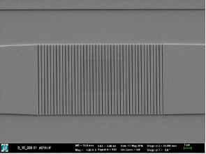
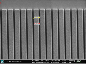
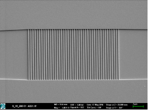
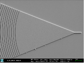
Fig. 1: SEM images of CSAR 62 nanostructures; parameters: film thickness 200 nm, dose 225 μC/cm2 at 100 kV, developer AR 600-546 for 3 minutes.
By repeatedly changing the developer solution and a final rinse with MIBK before use of the stopper IPA, the development step finally yielded defect- and particle-free structures. A particular challenge was in this case the writing and development of nano-sized perforation structures. With CSAR 62, the quite remarkable diameter of 67 nm could be realised, whereby the demanding structural element shows a highly regular pattern.
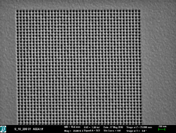
Fig. 2: SEM images of CSAR 62 nanostructures; parameters: film thickness 200 nm, dose 225 μC/cm2 at 100 kV, developer AR 600-546 for 3 minutes.
Related articles EBL positive
CSAR 62 related
3-layer system CSAR/PMMAcoMA/PMMA
3-layer system for T-gate CSAR/PMMAcoMA/PMMA
BOE etching of SiO2 with CSAR 62 mask
Collapse of extreme high-resolution e-beam resist structures
CSAR 62 Avoidance of particles during large-area exposures
CSAR 62 – Development at low temperatures
CSAR 62 – Experimental studies on new, sensitive developers
CSAR 62 lift-off for thick layers
CSAR 62 nanostructures written at 100 kV
CSAR 62 single layer lift-off system
Evaluation of various developers for e-beam exposed CSAR 62 layers (100 kV)
HF etching of GaAs with CSAR 62 masks
Manufacture of plasmonic nanostructures with CSAR 62
Use of CSAR 62 for the manufacture of nanostructures on GaAs substrates
