CSAR 62 lift-off for thick layers
For special applications in which metal layers with a thickness of a few hundred nanometres are to be generated by lift-off techniques, accordingly higher layers are needed. With AR-P 6200.13, 800 nm thick layers are obtained at a spin speed of 1000 rpm, and with AR-P 6200.18 even 1.5 µm thick films are realised.
The degree of the generated undercut could be specifically adjusted by increasing the exposure dose (Fig. 1-3). With this system, each user is able to choose the most favourable profile for the desired lift-off process. For the manufacture of nano-conducting paths with a metal height of a few 10 nm, still thin 100-200 nm resist layers should be used. In contrast allow „thick“ lift-off structures even the manufacture of columns with a height of a few 100 nm and an Ø <100 nm (e.g. nanowires).
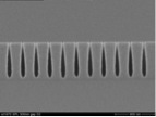
Fig. 1
AR-P 6200.13, 823 nm film,
dose: 1200 pC/cm
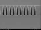
Fig. 2
AR-P 6200.13, 823 nm film,
dose: 1440 pC/cm
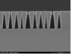
Fig. 3
AR-P 6200.13, 823 nm film,
dose: 1728 pC/cm
Since generally a considerable amount of polymer is dissolved in the developer during the development of thick layers, a brief rinsing with fresh developer and / or MIBK is highly recommended. The deposition of polymer residues or particles from the developer solution on the substrate can thus be effectively avoided. The subsequent stopping is carried out in AR 600-60.
Related articles EBL positive
CSAR 62 related
3-layer system CSAR/PMMAcoMA/PMMA
3-layer system for T-gate CSAR/PMMAcoMA/PMMA
BOE etching of SiO2 with CSAR 62 mask
Collapse of extreme high-resolution e-beam resist structures
CSAR 62 Avoidance of particles during large-area exposures
CSAR 62 – Development at low temperatures
CSAR 62 – Experimental studies on new, sensitive developers
CSAR 62 lift-off for thick layers
CSAR 62 nanostructures written at 100 kV
CSAR 62 single layer lift-off system
Evaluation of various developers for e-beam exposed CSAR 62 layers (100 kV)
HF etching of GaAs with CSAR 62 masks
Manufacture of plasmonic nanostructures with CSAR 62
Use of CSAR 62 for the manufacture of nanostructures on GaAs substrates
