CSAR 62 for EUV applications
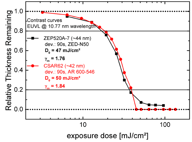
In addition to the use in e-beam lithography, the highly sensitive e-beam resist CSAR 62 can also be structured by exposure to UV radiation since the resist strongly absorbs UV radiation in the wavelength range of 190 – 240 nm. Similar to an irradiation with electrons, polymer bonds are also cleaved by the high-energy UV radiation. The fragmented polymer then shows a significantly increased solubility in the developer in the subsequent development step (positive patterning process). Previously unknown was however the ability to structure CSAR 62 with EUV radiation. Respective studies were conducted at the RWTH Aachen (Chair for Technology of Optical Systems) by Dipl. Ing. S. Brose. Layers of CSAR 62 (AR-P 6200.09) were exposed to EUV radiation (wavelength range of 10 – 16 nm) and compared with respect to contrast and sensitivity to a conventional patterning by electron beam irradiation. For CSAR 62 (layer thickness about 40 nm), a contrast of gamma = 1.8 with a sensitivity of 50 mJ/cm² was determined under EUV irradiation (developer AR 600-546, 5 minutes at room temperature). For e-beam exposure, a sensitivity of 85 µC/cm² was measured, with very similar contrast values. The observed contrast was almost identical for CSAR 62 and ZEP 520A-7, but a higher sensitivity could be measured for CSAR 62.
S. Brose, S. Danylyuk, J. Tempeler, H. Kim, P. Loosen, L. Juschkin; Proc. of SPIE 9776, Extreme Ultraviolet (EUV) Lithography VII, 97760R, (2016)
Related articles EBL positive
CSAR 62 related
3-layer system CSAR/PMMAcoMA/PMMA
3-layer system for T-gate CSAR/PMMAcoMA/PMMA
BOE etching of SiO2 with CSAR 62 mask
Collapse of extreme high-resolution e-beam resist structures
CSAR 62 Avoidance of particles during large-area exposures
CSAR 62 – Development at low temperatures
CSAR 62 – Experimental studies on new, sensitive developers
CSAR 62 lift-off for thick layers
CSAR 62 nanostructures written at 100 kV
CSAR 62 single layer lift-off system
Evaluation of various developers for e-beam exposed CSAR 62 layers (100 kV)
HF etching of GaAs with CSAR 62 masks
Manufacture of plasmonic nanostructures with CSAR 62
Use of CSAR 62 for the manufacture of nanostructures on GaAs substrates
