CSAR 62 – Development at low temperatures
The sensitivity of CSAR 62 is strongly influenced by the choice of the developer. In comparison to the standard developer AR 600-546, the sensitivity can be increased almost tenfold if AR 600-548 is used instead. The stronger developer however also causes a certain dark erosion which is tolerable to some degree: If for example consistently 10 % of the layer is lost, can this effect be compensated for in advance by using correspondingly thicker resist films. A development step at lower temperatures reduces the dark erosion considerably, but at the same time the sensitivity is decreased again. It thus comes down to the fact that an optimisation of the process is required. A gentler development at lower temperatures may also cause an increase in contrast and at the same time contribute to a lower edge roughness.
In the following, the sensitivities and resolutions of AR-P 6200.04 at 6 °C and 21 °C (developer AR 600-546) are shown. Due to the higher contrast at 6 °C, a maximum resolution of only 6 nm could be achieved. The doses used are listed in detail in the table (for example, # 1 = 45 µC/cm²).
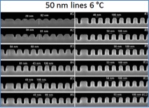
CSAR 62 structures at 6 °C, optimum dose 195 p C/cm

CSAR 62 structures at 21 °C, optimum dose 121 pC/cm
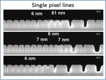
Maximum resolution of 6 nm at 235 pC/cm and 6 °C

Dose values of development experiments
The sensitivity can significantly be increased if the development is performed at higher temperatures, as first results demonstrated. With increasing developer temperature, CSAR 62 films show a significant increase in sensitivity after intensive exposure to UV light while the dark field loss still remains negligibly small, even at 40 °C.
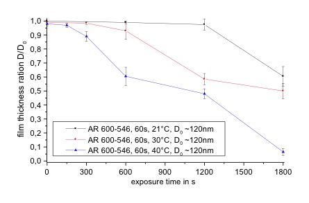
Development of UV-exposed CSAR 62 layers with AR 600-546: Influence of temperature
Related articles EBL positive
CSAR 62 related
3-layer system CSAR/PMMAcoMA/PMMA
3-layer system for T-gate CSAR/PMMAcoMA/PMMA
BOE etching of SiO2 with CSAR 62 mask
Collapse of extreme high-resolution e-beam resist structures
CSAR 62 Avoidance of particles during large-area exposures
CSAR 62 – Development at low temperatures
CSAR 62 – Experimental studies on new, sensitive developers
CSAR 62 lift-off for thick layers
CSAR 62 nanostructures written at 100 kV
CSAR 62 single layer lift-off system
Evaluation of various developers for e-beam exposed CSAR 62 layers (100 kV)
HF etching of GaAs with CSAR 62 masks
Manufacture of plasmonic nanostructures with CSAR 62
Use of CSAR 62 for the manufacture of nanostructures on GaAs substrates
